Solar Thin Film and Its Technical Advantages

Thin-film solar cells refer to thin films with thicknesses ranging from a few nanometers to tens of microns attached to the solar surface, which make thin-film cells lighter in weight. Thin-film solar cells are used in building-integrated photovoltaics as translucent photovoltaic glass materials that can be laminated to windows.

As a second-generation solar technology, thin-film technology is more affordable than the traditional first-generation c-Si technology, but is less efficient. Therefore, in recent years, people have also paid more attention to the development of sputtering materials and thin film coating technology, and are committed to improving the efficiency of thin film technology. And now it has improved significantly. Laboratory cell efficiencies for CdTe and CIGS are now over 21%, better than polysilicon, the main material currently used in most solar photovoltaic systems. And the life expectancy of thin-film solar cells is also extended to 20 years or more.

Thin film solar cells are made by depositing one or more thin layers or thin films of photovoltaic materials on a substrate such as glass, plastic or metal. In the deposition process, the coating source material used are usually sputtering targets or evaporation materials. Commonly used thin-film solar cell categories include cadmium telluride (CdTe) thin films, copper indium gallium selenide (CIGS) thin films, and gallium arsenide (GaTe) thin films.

The target materials corresponding to the three thin films mentioned above are important materials for the thin film coating of solar cells. Among them, cadmium telluride targets account for 50% of the solar market. On a life cycle basis, CdTe PV has the smallest carbon footprint, lowest water usage, and shortest energy payback time of all solar technologies. With an energy payback period of less than a year, CdTe can reduce carbon emissions faster without short-term energy shortages.

The CIGS sputtering target is composed of four metal elements, namely copper (Cu), indium (In), gallium (Ga) and selenium (Se), and it is also one of the representatives of commonly used targets in the solar industry. CIGS thin film has the advantages of strong light absorption, good power generation stability and high conversion efficiency, which can enable solar cells to generate electricity for a long time during the day and generate a large amount of electricity. CIGS has great advantages in photovoltaic building-integrated applications. At the same time, with the improvement of CIGS conversion efficiency, the self-sufficiency rate of CIGS as a photovoltaic building power supply built with glass curtain walls is also increasing.

GaAs thin-film solar cells have an efficiency of up to 28.8%, which is considered the highest efficiency of all thin films. Gallium arsenide is also resistant to damage from moisture, radiation and UV light. These properties make GaAs thin films an excellent choice for aerospace applications with increased UV and radiation.

For more information, please visit https://www.sputtertargets.net/.

Sources and Hazards of Industrial Waste Salt

Overview

Industrial waste salt mainly comes from industrial waste salt-containing organic matter and other toxic salt-containing waste liquids and solids produced in the production process of chemical, pharmaceutical, agrochemical and coal chemical industries. The main salt production links include reaction salts from mother liquor (process wastewater), neutralizing salts from acid-base chemical reactions, salting-out salts, and salt sludge from distillation residues.

The organic matter in waste salt has a complex composition, which has the characteristics of various types, complex components, numerous sources, high treatment costs, and great environmental hazards.

At present, waste salt is generally treated by building a warehouse and centralized temporary storage. Faced with high storage and management costs, it is difficult for enterprises to afford it, and it has become a “stuck neck” problem that restricts the development of enterprises.

At the same time, industrial waste salt is also an important chemical raw material. If the waste salt from chemical by-products can be recycled as industrial raw material salt, it can not only eliminate its pollution to the environment, but also make full use of salt resources to realize the resource and recycling of by-product salt.

In this context, the harmless and comprehensive utilization of waste salt has become an inevitable way to dispose of waste salt, and the main factor restricting its large-scale development is the removal of organic matter in waste salt.

Industrial Waste Salt

Sources and Characteristics of Industrial Waste Salt

There are many industries involved in the generation of waste salt. The types of waste salt produced include single waste salt, mixed salt and mixed salt (including impurities). According to the particularity of its production process and the difference in production links, the waste salt produced by different industries is quite different.

PESTICIDE PRODUCTION

Among them, pesticide production is the main industry for waste salt generation. Its main source is the production process of pesticide intermediates and original drugs. Pesticide waste salts contain a lot of organic matter, mainly halogenated hydrocarbons and benzene-based complex components, and the boiling point and thermal decomposition temperature of the organic compounds are within 200-600 °C.

PRINTING AND DYEING

The basic production raw materials in the printing and dyeing industry include naphthalene, anthraquinone, benzene, aniline and benzidine compounds. These substances are easy to chelate with metals, salts and other substances during the processing and production process, so the dye wastewater contains high concentrations of salts and heavy metals.

In the process of water treatment, the evaporation of high-salt wastewater will also indirectly generate waste salt. Such waste salts go through the oxidation and decomposition process of organic matter in the pre-water treatment process, so the residual organic matter is mostly refractory organic matter, which is difficult to remove.

COAL CHEMICAL INDUSTRY

The waste salt in the coal chemical industry mainly comes from the salt introduced in the production of demineralized water and circulating water, and the components are mainly simple salts such as NaCl and Na2SO4, without organic matter. In the chlor-alkali industry, NaOH, Cl2 and H2 are prepared by electrolysis of saturated NaCl solution, and a series of chemical products are produced by using them as raw materials. This kind of salt mud has a large output, the main component is NaCl, basically does not contain organic matter, and has high recycling value.

In addition, the petrochemical, coal chemical, Chlor-alkali industry, metallurgy and other industries also produce waste salt, but the organic content is relatively low, and the processing difficulty is relatively small.

Treatment Methods

WET PROCESS

Wet treatment first dissolves waste salt in water, and degrades organic pollutants through deep oxidation technology in the field of water treatment to achieve harmlessness of waste salt. Commonly used organic oxidation technologies include advanced oxidation, wet catalytic oxidation and hydrothermal oxidation.

DRY METHOD

Dry disposal of industrial waste salt mainly includes incineration, high-temperature thermal melting, and organic carbonization pyrolysis. Because of its long-term environmental hazards, occupation of land resources and legal risks, the safe landfill method can no longer meet the needs of waste salt disposal.

We will also write related articles to introduce these two methods in detail, please pay attention to our later updated articles. For more information, please visit https://www.sputtertargets.net/.
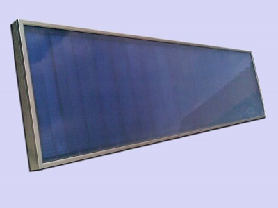
Classification of Molybdenum Target Materials

Molybdenum sputtering targets perform the same as their source material (pure molybdenum or molybdenum alloy). Molybdenum is a metallic element mainly used in steel, where it improves the strength, hardness, weldability and toughness of alloys, as well as high temperature and corrosion resistance. Molybdenum targets are one of the important sputtering materials and are used in aerospace, semiconductor, solar and many other applications.

Different Shapes of Sputtering Target

Classify by Shape of Molybdenum Target

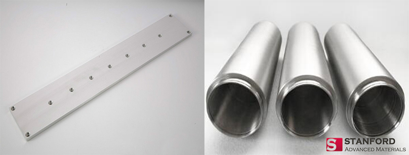
According to the shape of the target, the molybdenum target can be divided into square molybdenum target, circular molybdenum target, molybdenum plate target, rotatory molybdenum target, and molybdenum tube target.

The square molybdenum target has the characteristics of high melting point, high electrical conductivity, low impedance, good corrosion resistance and good environmental performance. It is the most widely used planar molybdenum target.

The circular molybdenum target, or the disc molybdenum target, also has a wide range of applications, which can form films on various types of substrates, and these films can be widely used in electronic components and electronic products.

Molybdenum plate target common thickness is 0.09 inch ~ 3 inch and the surface shows silver-gray metallic luster. Common Specifications (mm) is BCM = 9.9 (0.3-10) (60-400) 800 or bigger.

The rotatory molybdenum target is a rotatable sputtering target that is usually cylindrical and has a fixed magnet so that it will rotate at a low speed during operation.

The length of the molybdenum tube target is generally ≤3000mmm, and the outer diameter is ≤250mm. The wall thickness is 3-25 mm and the flatness is 0.1 mm. In addition, its shape is tubular and the surface shows a silver metallic luster.

Classify by Applications of Molybdenum Target

According to its application, the molybdenum target can be divided into the X-ray molybdenum target, the coated molybdenum target, and etc. Stanford Advanced Materials offers a wide range of high performance, high quality molybdenum targets.

Coated molybdenum target has good properties, including excellent high temperature performance, high temperature physical strength, high elastic modulus, excellent thermal conductivity and corrosion resistance and other properties, so commonly used in the field of coatings, as coating materials.

X-ray molybdenum targets are commonly used in the medical field for breast examination of women. X-ray mammography as a non-invasive method can more fully and accurately reflect the structure of the entire breast.

If you have any interest in molybdenum metal targets, please visit our website at https://www.sputtertargets.net/.

Study on Preparation Methods of Magnesium Film Materials

Thin-film is a rapidly developing material in the field of modern material science and technology, and there are many methods for its preparation. This article introduces several methods for preparing thin films, focusing on magnetron sputtering and ion beam sputtering deposition, and using magnesium sputtering targets as raw materials to prepare magnesium thin films.

Magnesium is in a diagonal position with lithium in the periodic table of the elements, has similar chemical properties to lithium, and has some electrochemical properties better than lithium, which can meet the needs of power batteries. Magnesium batteries have many advantages such as low cost, non-toxicity, no pollution, stable discharge voltage, high specific energy, high specific power, rich resources, and renewable. However, magnesium batteries have not been widely used. One of the main reasons is that magnesium is severely polarized and corroded in the electrolyte, making it unable to meet the applicable standards and difficult to meet the actual requirements. Research on magnesium thin-film materials can help improve this defect of magnesium batteries.

Principle of magnetron sputtering coating

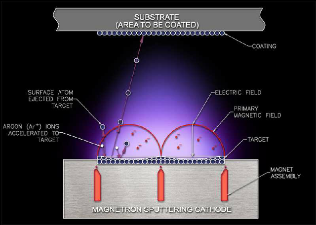
Sputter deposition is the process whereby particles of sputtering materials are sputtered out and deposited on a substrate to form a film. Since ions are charged particles, we can add magnetic fields to control their speed and behavior. And that’s how its name “magnetron sputtering” comes from.

Under the action of an electric field of several hundred to several thousand electron volts, the plasma is accelerated and obtained sufficient force to bombard the cathode, causing the atoms of the solid sputtering target to be ejected in a typical line-of-sight cosine distribution. These atoms will condense on the surface of the substrate to form a thin film.

Ion beam sputtering coating

Ion beam sputtering (IBS), or ion beam deposition (IBD), is a thin film deposition technology that uses an ion source to deposit a sputtering target onto a substrate to produce the highest quality films with excellent precision. Compared to other PVD technologies, ion beam sputtering is more accurate and can accurately control the thickness of the substrate. As shown below, an IBS system usually includes the ion source, the target material, and the substrate. The ion beam, usually generated by the ion gun, is focused on the sputtering target, and the sputtered target material finally deposits onto the substrate to create a film.

Preparation of magnesium film material

In the preparation of magnesium-thin films, magnetron sputtering is a very good choice. This method has the advantages of high speed, low temperature and low damage. The deposited layer is uniform, dense, has small pinholes, high purity, and has strong adhesion. These advantages are the key to the quality of magnesium films. The selected targets are high-purity powder-pressed magnesium sputtering targets and magnesium alloy sputter targets.

For more information about thin-film coating, please visit https://www.sputtertargets.net/.

Seven Sputtering Targets and Their applications

Tantalum is used as a barrier layer on silicon wafers for semiconductor production, and tantalum is used in all modern electronic products. Mobile phones, DVD and Blu-ray players, laptops, etc. Car electronics and even game consoles contain tantalum.

Niobium is commonly used in electronic products and its properties are similar to tantalum. Niobium has corrosion resistance due to its oxide film and is considered a superconductor.

Titanium has the characteristics of light weight and corrosion resistance, and can be used in various conventional products including watches, notebook computers and bicycles. Titanium is commonly used for wear resistance and aesthetic design, but can also be used for semiconductor and optical coatings.

Read more: Everything You Need to Know About Titanium Sputtering Target

Tungsten film is a decorative coating, due to its thermal, physical and mechanical properties (such as high melting point
And thermal conductivity) and widely used.

Molybdenum has a lower density and a consistent price, and can be used to replace tungsten. It is usually used to coat solar panel cells.

black and white solar panels

It is often used as an insulator for semiconductors, as well as surface hardness and protective layer. As an element with a high dielectric constant, it can improve the performance of certain electronic devices.

This target material is most commonly used in the production of silicon solar cells.

What are the advantages of carbon fiber composite materials used in aeroplanes?

Carbon fiber is a kind of special fiber mainly composed of carbon element and generally contains more than 90% carbon. Carbon fiber has the characteristics of high-temperature resistance, friction resistance, electrical conductivity, thermal conductivity, and corrosion resistance to general carbon materials. However, unlike ordinary carbon materials, its shape has significant anisotropy, and it shows strong strength along the fiber axis.

With its own unique advantages, carbon fiber reinforced composites have also been widely used in the aircraft manufacturing industry. Especially for smaller airplanes, carbon fiber composites are the best choice.

As a kind of carbon fiber, carbon fiber composite material has a wide range of applications in many fields due to its characteristics of high strength, lightweight, stable chemical properties, high-temperature resistance, and strong durability. Applying it to the fuselage and wings of an airplane can reduce the weight of the airplane by about 40%, and its crawling ability can be increased by 1.8 times compared with the airplane of ordinary materials.

Compared with military and civil aircraft, model aircraft are smaller in size, shorter in-flight operation time, and the working environment is relatively better. Applying carbon fiber composite materials to model aircraft can increase their service life, so they can be applied to the harsh environments.

aircraft concord

The application of carbon fiber composite materials to airplane aircraft can not only reduce the mass of the airplane but also increase the strength tolerance range of the airplane aircraft to a certain extent. The fuselage and propeller made of carbon fiber composite materials reduce the weight of the airplane while increasing its strength, thereby reducing its volume.

With the continuous development of the aerospace industry, the demand for carbon fiber composites is increasing. At the same time, people have put forward higher requirements for the quality of carbon fiber composite materials, which in a certain sense promotes the development of carbon fiber composite materials in the direction of multifunctionality, low cost and high performance.

Compared with glass fiber, the application cost of carbon fiber is also relatively high, and it is more difficult to promote and use it in a wide range. From the current situation, the price of carbon fiber materials has not only declined, but also shown an upward trend. To solve this problem, new processes must be studied to reduce the cost of carbon fiber composites.

Carbon fiber materials can also be made into the carbon sputtering target for aviation coatings. Stanford Advanced Materials provides high-quality sputtering targets and evaporation materials. Please visit https://www.sputtertargets.net for more information.

Preparation of Molybdenum Sputtering Targets by Powder Metallurgy

Molybdenum film has many advantages such as good electrical conductivity and thermal stability, chemical resistance, and low thermal expansion coefficient. It has been widely used in solar power generation, computer circuits, flat panel displays, storage media, and other aspects.

The magnetron sputtering technology has many advantages such as densely rented thin films, low surface roughness, good film-base bonding force, high deposition rate, low substrate temperature, and convenient deposition of thin films with high melting points. It is currently the main method for preparing molybdenum films using molybdenum sputtering targets.

Previous studies have shown that the choice of different magnetron sputtering equipment and process parameters (target current, target power, gas pressure, sputtering time, etc.) should also have a close relationship with the differences in the structure and performance of the sputtered thin films.

molybdenum target powder metallurgy

The electronic display industry’s technical requirements for sputtering targets mainly include indicators such as chemical purity, density, grain size and size distribution, grain orientation and orientation distribution. Recent studies have shown that the smaller the grain size of the target, the higher the sputtering rate; the more uniform the grain size distribution of the target, the easier it is to obtain a sputtered film with uniform thickness.

Since molybdenum is a high melting point (2620 ° C) metal. Powder metallurgy is the main method for preparing molybdenum targets. The process mainly includes the steps of milling, pressing, and sintering.

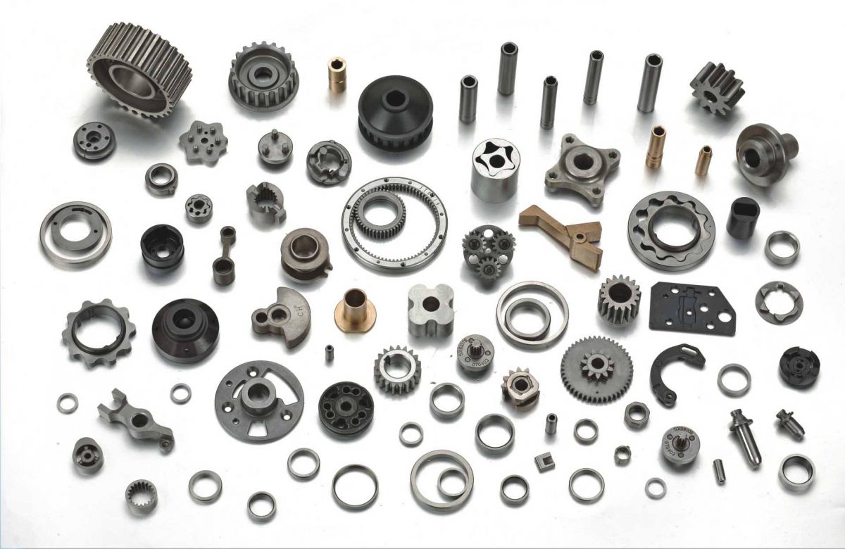
The powder metallurgy method is a technical method in which metal powders, alloy powders or mixed powders of metals and non-metals are directly made into various products through pressing, sintering and other processes. The main feature of this method is that it can produce special material products that are difficult to achieve or cannot be manufactured by conventional metallurgical methods or material processing methods, such as parts of machines made of refractory tungsten and molybdenum metals.

The main features of powder metallurgy are: the raw materials can be directly manufactured into qualified products according to the shape and size requirements of parts and components without mechanical cutting or slight cutting; suitable for mass production and high efficiency; Less waste during production and high utilization of raw materials. This method has been widely used in the automotive industry, energy industry, chemical industry, national defense industry, and aviation and aerospace industries.

For more information, please visit https://www.sputtertargets.net/.
Advantages of Sputtering Deposition and Vacuum Evaporation

For all devices, there is a need to go from semiconductor to metal. Thus we need a means to deposit metals, also called film coating. There are currently several methods for depositing metal thin film layers, and many of these techniques for metal deposition can also be used to deposit other materials.

1.) Physical Vapor Deposition (PVD)

2.) Electrochemical techniques

3.) Chemical Vapor Deposition (CVD)

This passage will talk about the advantages of two PVD methods: Sputtering and evaporation.

Sputtering Deposition

magnetron-sputtering-system
Magnetron Sputtering System

The plasma under high pressure is used to “sputter” metal atoms out of the “target”. These high-energy atoms are deposited on a wafer near the sputtering target material. Higher pressures result in better step coverage due to more random angular delivery. The excess energy of the ions also helps increase surface mobility (the movement of atoms on the surface).

Advantages: Better step coverage, less radiation damage than E-beam evaporation, easier to deposit alloys.

Disadvantages: Some plasma damage including implanted argon. Good for ohmics, not Schottky diodes.

Vacuum Evaporation

Evaporation (PVD)
Evaporation (PVD)

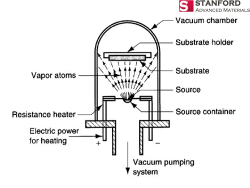
Evaporation is based on the concept that there exists a finite “vapor pressure” above any material. The material either sublimes (direct solid to vapor transition) or evaporates (liquid to vapor transition).

Advantages: Highest purity (Good for Schottky contacts) due to low pressures.

Disadvantages: Poor step coverage, forming alloys can be difficult, lower throughput due to low vacuum.

PVD Film Morphology

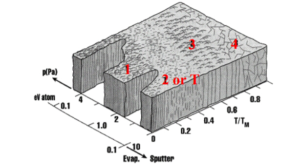
The three zone model of film deposition as proposed by Movchan and Demchishin

1.) Porous and/or Amorphous —> Results from poor surface mobility =low temperature, low ion energy (low RF power/DC bias or higher pressures=less acceleration between collisions).

2.) “T-zone”: Small grain polycrystalline, dense, smooth and high reflectance (the sweet spot for most metal processes) Results from higher surface mobility =higher temperature or ion energy

3.) Further increases in surface mobility result in columnar grains that have rough surfaces. These rough surfaces lead to poor coverage in later steps.

4.) Still further increases in surface mobility result in large (non-columnar) grains. These grains can be good for diffusion barriers (less grain boundary diffusion due to fewer grains) but pose problems for lithography due to light scatter off of large grains, and tend to be more rigid leading to more failures in electrical lines.

For more information, please visit https://www.sputtertargets.net/.
Advantages of Investing in Platinum and Palladium Precious Metals

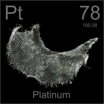
Platinum and palladium are in the class of precious metals just like gold and silver in spite of little information concerning their investments. The difference is that they are not in form of currency because they are in form of industrial metal, and belong to a group called platinum metals group.

Platinum

The fact that platinum is not a monetary metal confers advantages and disadvantages alike. First, it can be affected by demand issues due to its industrial nature and hence suffer massive price fluctuations sue to speculation. Secondly, it does not have the global attraction that gold and silver have as monetary metals. However, the fact that it non-monetary ensures that it is not targeted for confiscation as is the case with silver and gold. Second, the historic hart of the metal has shown that its price goes hand in hand with gold value over time even though it is more of an industrial metal. This tells you that it is a worth investment.

Related: Platinum Sputtering Target

Ways to Buy Platinum

There are a number of reputable dealers that can be contacted online. These dealers have established stores in Hong Kong, Switzerland or London. You can buy in small quantities from independent but reputable companies. For bulk buying, ensure that there is an arrangement for adequate storage because safety is of great importance. Second, you can explore mints that can produce bullion coins in the U.S, Canada, Australia, and China. The coins are available in the denominations between a tenth of an ounce and one troy ounce. Collectors tend to be more expensive than mints since most coins are regarded as collector’s items. Finally, you can consider collecting old or scrap platinum jewelry from second hand or coin shops. Another advantage of buying platinum jewelry is the authenticity and purity that comes with them.

Palladium

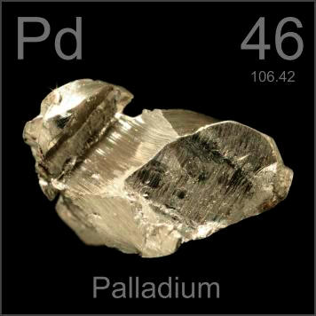
Palladium has lesser value compared to platinum and heavily relies on industrial demand behavior. For instance, palladium is expected to be a key part of the cold fusion technology that all industrialized nations are looking up to for energy solutions. Sharp investors are eager to become part of this booming technology by investing in palladium.

Related: Palladium Sputtering Target

Buying Palladium

An investor should look at reputable independent companies to buy palladium. It is available in bars and coins. For investors that want to start small, you can start with ounces or even smaller quantities.

For more information about precious metals, please visit https://www.sputtertargets.net/.

Silicon Wafer: 4 Types of Wet Cleaning Method

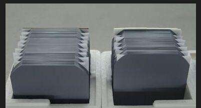
After the silicon wafer is processed by different processes such as slicing, chamfering, grinding, surface treatment, polishing, and epitaxy, the surface has been seriously stained. The purpose of cleaning the Si wafer is to remove particles, metal ions and organic substances on the surface of the silicon wafer.

Semiconductor-Silicon-Wafers

Wet cleaning uses chemical solvents with strong corrosive and oxidizing properties, such as H2SO4, H2O2, DHF, NH3•H2O, etc. The impurity particles on the surface of the silicon wafer react with the solvent to form soluble substances and gases. In order to improve the cleaning effect, it is possible to use mega-acoustic, heating, vacuum and other technical means, and finally use ultra-pure water to clean the surface of the silicon wafer to obtain a silicon wafer that meets the cleanliness requirements.

There are several methods for wet cleaning the silicon semiconductor wafer:

RCA Cleaning for Silicon Wafer

Kern et al. proposed the RCA cleaning method in 1965. According to the SPM, DHF, SC-1, and SC-2 sequences, the RCA cleaning method basically satisfies the requirements of most wafer cleanliness. Cleaning the silicon wafers by this method not only improves the cleaning efficiency, reduces the cost, saves time, obtains excellent surface cleanliness, but also improves the electrochemical performance of the Si wafer.

Ultrasonic Cleaning for Silicon Wafer

Ultrasonic cleaning is a cleaning method widely used in the semiconductor industry. The method has the advantages of good cleaning effect, simple operation, and can be removed for complicated devices and containers; but the method also has the disadvantages of high noise and easy breakage of the transducer.

This method can effectively remove organic, particulate, and metal ion impurities on the surface of the silicon wafer by utilizing the mechanical action of high-frequency sound waves, the cavitation effect of the solution, and the complexation reaction of chemical reagents. Using a similar method, BongKyun et al. used a 0.83 MHz megasonic wave to clean the silicon wafer, which is more excellent and can remove particulate impurities below 0.3 μm.

Silicon Wafer Wet Cleaning

Double Flow Spray for Silicon Wafer

The dual-flow atomizing nozzle cleans the silicon wafer by using a nozzle to scan the silicon wafer back and forth with the rotating arm, and the silicon wafer rotates clockwise. The dual-flow nozzle uses a high-pressure, high-speed jet of gas to impinge a vulgar flow of liquid, destroying the surface tension of the liquid and the van der Waals bond and hydrogen bond between the liquid molecules, causing the liquid to atomize and become nanometer-sized droplets, which are ejected at high speed through the nozzle under the action of high pressure air.

Ozone Microbubble Method for Silicon Wafer

The high activity and strong oxidizing properties of ozone can remove organic and particulate impurities on the surface of the Si wafers. Ozone is dissolved in water to form a highly reactive OH group, and the OH group chemically reacts with the organic substance to remove organic impurities on the surface of the silicon semiconductor wafer. At the same time, the surface of the silicon product is covered with an atomic-level smooth oxide film, which effectively isolates the re-adsorption of impurities.

This method has an excellent cleaning effect, basically removes organic and particulate impurities, and meets the requirements of general silicon wafer cleanliness. At the same time, ozone microbubble cleaning produces less polluting waste and high cleaning efficiency, and can be used for cleaning large-scale circuits, silicon wafers and LEDs.

For more information, please visit https://www.sputtertargets.net/.