Indium Tin Oxide (ITO) in Liquid Crystal Displays (LCDs): Key to Bright, Efficient Screens

Indium Tin Oxide (ITO) is a vital material in the world of modern displays, particularly in Liquid Crystal Displays (LCDs). Found in televisions, computer monitors, smartphones, and a myriad of other electronic devices, ITO serves as a transparent electrode, a role that is central to creating clear, bright, and energy-efficient screens. Understanding how ITO works and why it is essential in LCDs can provide insight into the technology behind our daily displays.

The Function of ITO in LCD Technology

At the core of every LCD is a layer of liquid crystals, sandwiched between two glass substrates. These liquid crystals do not produce light by themselves; instead, they manipulate external light to form images. This is where Indium Tin Oxide (ITO) comes in.

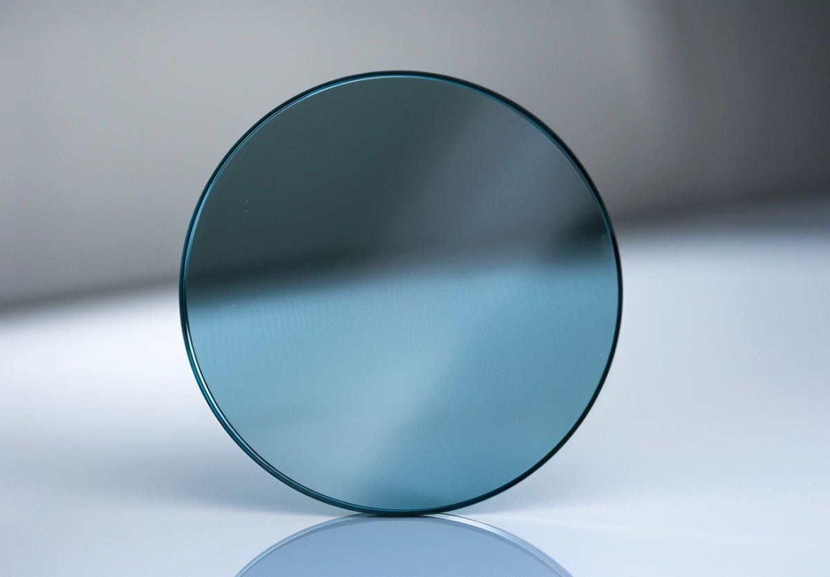
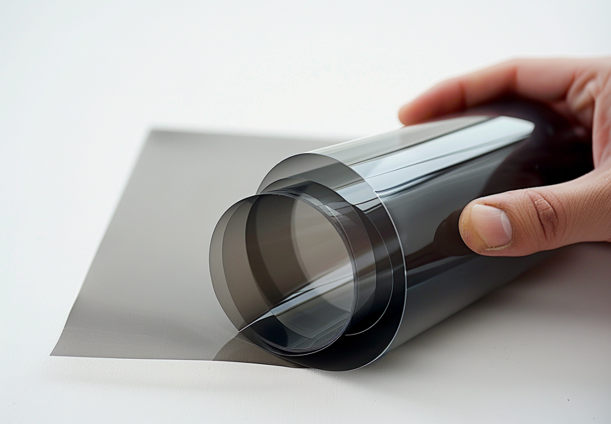
ITO is a compound that combines indium oxide and tin oxide, forming a material that is both conductive and transparent. When applied as a thin film to one or both glass substrates in an LCD, it acts as an electrode that conducts electricity while allowing light to pass through. This dual property is what makes ITO so valuable in display technology.

An electric current passing through the ITO layer generates an electric field that affects the orientation of the liquid crystals. Depending on their orientation, the liquid crystals either block or allow light to pass through. By carefully controlling the voltage applied across the ITO electrodes, manufacturers can adjust the liquid crystals’ alignment, creating varying shades, colors, and levels of brightness that form the images you see on your screen.

Benefits of Using ITO in LCDs

  1. High Transparency and Clarity: The primary advantage of ITO in LCDs is its high level of transparency. This property ensures that maximum light reaches the viewer without being absorbed or reflected by the conductive layer. As a result, LCDs using ITO provide a bright, clear display that is easy to read even in well-lit environments. The glare reduction further enhances visibility and readability, making screens more comfortable for prolonged use.
  2. Improved Contrast and Color Accuracy: By controlling the orientation of the liquid crystals precisely, ITO allows for a high contrast ratio, where the difference between the darkest blacks and the brightest whites is maximized. This precise control also enhances color accuracy, making colors more vibrant and true to life. The ability to finely adjust the electric field helps create smooth gradients and sharp images, improving the overall visual experience.
  3. Energy Efficiency: ITO contributes significantly to the energy efficiency of LCDs. Because it allows for precise control over the liquid crystals with minimal electrical input, LCDs require less power to operate. This is particularly important in battery-powered devices such as laptops, tablets, and smartphones, where energy consumption directly impacts battery life. The energy savings provided by ITO make these devices more sustainable by reducing their energy footprint.
  4. Durability and Reliability: In addition to its optical and electrical properties, ITO is also highly durable and resistant to environmental factors such as moisture and temperature fluctuations. This resilience ensures that displays maintain their performance and longevity, even under challenging conditions. For manufacturers, this means fewer defects and returns, and for consumers, it translates to a longer-lasting display with consistent performance over time.

Applications Beyond LCDs

While ITO is best known for its use in LCDs, its applications extend to other types of displays and devices as well. ITO is commonly used in organic light-emitting diode (OLED) displays, touch screens, and photovoltaic cells, where its transparent and conductive properties are equally advantageous. As display technology continues to evolve, ITO remains a critical material for achieving the best performance, efficiency, and reliability.

Read more: How Indium Tin Oxide (ITO) Improves Flat-Panel Displays

Conclusion

Indium Tin Oxide is an essential material in the production of modern LCDs, offering benefits that range from high transparency and clarity to improved energy efficiency and durability. Its unique combination of properties makes it invaluable in creating bright, vivid, and efficient displays. As the technology landscape continues to shift, ITO’s contributions will remain at the forefront of display innovation, enabling clearer, more energy-efficient screens in the devices we rely on every day.

Get more info on SAM’s website.

What’s Next for ITO and Iron Sputtering Target Technology?

Sputtering targets are materials used to make thin films for many high-tech products, like those in electronics, cars, and renewable energy. Two important types are Indium Tin Oxide (ITO) and iron sputtering targets, which help create coatings that conduct electricity and protect surfaces. As technology changes, new trends are making these materials more efficient, affordable, and better for the environment. Here’s what we can expect in the future.

Making Better Use of Materials

One of the biggest problems in sputtering is the waste of materials. Current sputtering methods often use only a small part of the target, which leads to waste and higher costs.

New Ways to Reduce Waste

To fix this, new methods are being developed to use more of the target material. For example, rotating targets and better magnetron designs can help spread out the use of the material more evenly. This means less waste and lower costs. New power technologies can also make the sputtering process use less energy. These changes can help both ITO and iron sputtering be more efficient and environmentally friendly.

Finding New Materials to Use

ITO is popular for things like touchscreens, displays, and solar panels because it is clear and conducts electricity well. But it depends on indium, which is a rare and expensive metal.

Looking for Other Options

Scientists are looking for other materials that can do the same job as ITO but are easier to find and less expensive. Some good options might be aluminum-doped zinc oxide (AZO) or graphene-based materials. These materials can offer similar benefits without the high cost or supply problems of indium. This shift could lead to new designs and uses for future devices.

Improving How Sputtering Targets Are Made

The quality of sputtering targets affects how well the thin films they create will perform. So, better ways to make these targets are becoming more important.

Better Production Techniques

New methods in powder metallurgy can help create a more uniform material with fewer impurities. Improved bonding methods can make the targets stronger and less likely to have defects. Also, new casting techniques can help produce larger and more consistent targets, leading to fewer mistakes and better-quality films. These improvements are important for products like screens, solar cells, and electronics that need high-performance coatings.

Focusing on Recycling and Sustainability

With growing concerns about the environment, recycling sputtering targets, especially those with rare materials like indium, are becoming more important.

Developing New Recycling Methods

Future trends will likely focus on better recycling techniques to recover valuable materials from used targets. Improved chemical and mechanical methods could make it easier to get back indium and other rare elements. This approach will reduce waste and lower costs, while also supporting a circular economy where materials are reused, reducing the need for new resources.

Using Digital Technology

Digital tools are changing how sputtering is done by using technologies like IoT (Internet of Things), AI (Artificial Intelligence), and machine learning.

Smarter Manufacturing

These tools help control the sputtering process in real time, monitor equipment, and predict when maintenance is needed, preventing breakdowns. For ITO and iron sputtering, this means better production, less downtime, and higher quality. By using data analysis, these technologies can also help find new ways to improve the process, making it more adaptable to changing needs.

Finding New Uses in the Market

As new uses for sputtered films are discovered, demand for ITO and iron sputtering targets is likely to grow in different markets.

Expanding into New Areas

For example, ITO is becoming more popular in flexible electronics and wearable devices that need materials to be both flexible and conductive. At the same time, iron sputtering targets are being used in energy storage technologies, like batteries, to improve performance and lifespan. As these markets expand, so will the need for ITO and iron-sputtering targets, opening up new opportunities.

Conclusion

At Stanford Advanced Materials, we aim to lead in these future trends. With our experience in high-quality sputtering targets, we are ready to meet the changing needs of our customers and support new technology. Check out our range of sputtering targets today to see how we can help you stay ahead in this evolving industry.

Introducing Transparent Conductive Oxides: A Gateway to Advanced Technologies

Transparent conductive oxides (TCOs) are a class of materials that have revolutionized various high-tech industries, from consumer electronics to renewable energy. These materials uniquely combine optical transparency and electrical conductivity, making them indispensable in modern technology. This article explores the fundamental properties of TCOs, their applications, and a detailed look at one of the most prominent TCOs—Indium Tin Oxide (ITO).

Understanding Transparent Conductive Oxides

Transparent conductive oxides are inorganic materials that possess both high electrical conductivity and optical transparency in the visible spectrum. This combination is unusual because materials that conduct electricity well are typically opaque. TCOs achieve this by having wide band gaps, which allow them to be transparent to visible light, while their electrical conductivity is facilitated by free electrons or holes.

Key Properties of TCOs

  1. Optical Transparency: TCOs must have a band gap greater than 3.1 eV to ensure transparency in the visible range.
  2. Electrical Conductivity: This is achieved through doping, where additional elements introduce free carriers (electrons or holes) to the material.
  3. Chemical Stability: TCOs need to maintain their properties under various environmental conditions, including exposure to moisture and varying temperatures.

Applications of Transparent Conductive Oxides

The unique properties of TCOs make them suitable for a wide range of applications:

  1. Display Technology: TCOs are used in liquid crystal displays (LCDs), organic light-emitting diode (OLED) displays, and touch screens.
  2. Solar Cells: TCOs are crucial in photovoltaic cells, particularly in the front electrodes of thin-film solar cells.
  3. Smart Windows: These windows can change their light transmission properties in response to an external stimulus, such as voltage or light.
  4. Flexible Electronics: TCOs enable the development of bendable and foldable electronic devices, opening new possibilities in wearable technology.

Spotlight on Indium Tin Oxide (ITO)

Indium Tin Oxide (ITO) is the most widely used TCO due to its excellent balance of transparency and conductivity. Comprising indium oxide (In2O3) and tin oxide (SnO2) in varying proportions, ITO is favored for several key reasons:

Related: ITO vs. FTO Films as Transparent Conductive Oxides (TCOs)

Properties of ITO

  1. High Transparency: ITO films can achieve over 85% transparency in the visible spectrum.
  2. Low Electrical Resistance: With a resistivity as low as 10^-4 ohm-cm, ITO is highly conductive.
  3. Ease of Deposition: ITO can be deposited using various techniques such as sputtering and electron beam evaporation, making it versatile for different manufacturing processes.

Applications of ITO

  1. Flat-Panel Displays: ITO is extensively used in the electrodes of LCDs and OLEDs due to its excellent transparency and conductivity.
  2. Touch Panels: The conductive and transparent nature of ITO makes it ideal for touch screen technology.
  3. Solar Cells: ITO is used as a front contact in various types of solar cells, contributing to efficient light absorption and conversion.
  4. Light Emitting Diodes (LEDs): ITO layers are used in LEDs to improve their performance and efficiency.

Challenges and Alternatives

Despite its widespread use, ITO faces challenges such as the high cost of indium and brittleness, which limits its application in flexible electronics. Researchers are actively exploring alternative materials like aluminum-doped zinc oxide (AZO) and graphene to address these limitations.

Future Prospects of Transparent Conductive Oxides

The demand for advanced TCOs is expected to grow with the increasing need for energy-efficient technologies and the proliferation of smart devices. Innovations in material science are likely to yield new TCOs with enhanced properties and broader applications, potentially overcoming the current limitations of materials like ITO.

Conclusion

Transparent conductive oxides, particularly Indium Tin Oxide, play a critical role in the development of modern technology. As research continues to advance, we can anticipate even more innovative applications and materials that will drive the next generation of electronic and optoelectronic devices. Understanding and improving TCOs is essential for the continued evolution of technologies that shape our everyday lives.

Comparing the Advantages and Disadvantages of PVD and CVD

Introduction

Physical Vapor Deposition (PVD) and Chemical Vapor Deposition (CVD) are essential coating techniques used in various industries. Both methods offer distinct advantages and drawbacks, influencing their suitability for specific applications. This article provides an integrated comparison of PVD and CVD, highlighting their respective strengths and weaknesses.

Understanding PVD and CVD

PVD involves the physical transfer of material from a source to a substrate through processes like sputtering or evaporation. Typically operating at lower temperatures, PVD is advantageous for coating heat-sensitive materials. In contrast, CVD relies on chemical reactions to deposit a thin film on the substrate. This process occurs at higher temperatures and involves gaseous precursors that decompose or react to form the coating.

Advantages and Disadvantages of PVD

PVD is well-regarded for its lower temperature requirements, making it ideal for applications involving heat-sensitive substrates. The process is environmentally friendly, producing minimal toxic by-products, and it results in high-purity coatings with excellent adhesion. However, PVD has its limitations. The need for a direct line of sight between the material source and the substrate restricts its effectiveness on complex geometries. Additionally, the deposition rates in PVD are generally slower than those in CVD, which can impact efficiency in large-scale productions. Despite the lower temperatures, certain PVD processes may still negatively affect heat-sensitive substrates, necessitating careful process control.

Advantages and Disadvantages of CVD

CVD excels in providing uniform coatings, even on substrates with intricate shapes. This uniformity makes it advantageous for applications where coating conformity is critical. CVD also offers higher deposition rates, making it efficient for mass production and reducing overall processing time and costs. Furthermore, CVD can deposit a diverse range of materials, including metals, ceramics, and polymers, offering versatility in various industrial applications. However, CVD’s high-temperature requirements can limit its use with temperature-sensitive substrates. The process also produces toxic by-products, necessitating stringent safety protocols and effective waste management systems. Additionally, CVD systems are typically more complex and costly to operate and maintain compared to PVD, which can be a significant drawback for smaller operations.

Applications

PVD finds extensive use in the electronics industry, creating thin films for semiconductors and other electronic components. It is also employed in decorative coatings, enhancing the appearance and durability of consumer goods like watches and jewelry. In the tooling industry, PVD provides hard coatings for cutting tools, significantly improving their durability and performance by reducing wear and friction.

CVD is commonly used in aerospace for protective coatings on turbine blades and other components exposed to high temperatures and harsh environments. In the medical field, CVD enhances the biocompatibility of implants and medical tools, making them safer and more effective for patient use. The optics industry uses CVD to produce anti-reflective and other specialized coatings for optical instruments, improving their performance and longevity.

Conclusion

Deciding between PVD and CVD depends on specific application requirements, including temperature tolerance, coating uniformity, and production scale. PVD is favored for its lower temperature operations, environmental benefits, and high-purity coatings. Conversely, CVD is preferred for its efficiency in providing uniform coatings and material versatility, despite its higher operational complexity and cost. Understanding these nuances is crucial for selecting the optimal coating technique for your industrial applications, ensuring both performance and cost-effectiveness.

For further detailed information, you can read this article PVD vs. CVD: In-depth Comparison.

Lithium Battery Technology-An Overview

What is a lithium battery?

Contrary to some beliefs, lithium batteries are not exclusively composed of metallic lithium. Instead, they encompass a broad category of batteries that can be generally divided into two types: lithium metal batteries and lithium-ion batteries. Typically, the term “lithium battery” refers to batteries that use a lithium metal or lithium alloy as the anode and a non-aqueous electrolyte.

One of the most commonly used lithium-based chemicals in renewable energy applications is lithium iron phosphate (LiFePO4). LiFePO4 batteries are known for their high safety standards, excellent thermal stability, high rated current capacity, and long cycle life. These characteristics make them suitable for various applications, including electric vehicles, energy storage systems, and portable electronics.

Lithium battery2

Advantages

Lithium batteries offer several advantages over traditional batteries like lead-acid, nickel-chrome, and nickel-hydrogen batteries:

  1. Environmental Impact: Lithium batteries do not contain harmful heavy metals such as lead, mercury, or cadmium, making them more environmentally friendly. Their electrolytes are typically organic solvents and lithium salts, which are mostly non-toxic or low-toxic, resulting in relatively low pollution.
  2. Safety: Lithium batteries do not pose a risk of exposure to corrosive electrolytes like sulfuric acid or potassium hydroxide. They generally do not present an explosion hazard even when stored in confined spaces, and their well-designed systems eliminate the need for active cooling or ventilation.
  3. Longevity: Lithium batteries have an exceptionally long cycle life, with some manufacturers guaranteeing up to 10,000 cycles. This long lifespan makes them a cost-effective solution in the long run.
  4. Performance: Lithium batteries provide high energy density, allowing for compact and lightweight battery designs. They also offer high efficiency, quick charging times, and a wide operating temperature range, making them suitable for various demanding applications.
  5. Maintenance: Unlike some traditional batteries, lithium batteries require minimal maintenance, which reduces the total cost of ownership.

Application

The advent of microelectronics technology in the twentieth century has led to an increased demand for miniaturized devices with high-performance power supplies. As a result, lithium batteries have become widely used in various fields:

1. Semiconductor Manufacturing:
  • Wafer Processing: Utilized in semiconductor wafer processing equipment for applications such as epitaxy, chemical vapor deposition (CVD), and physical vapor deposition (PVD).
  • Test Equipment: Employed in test and measurement equipment for semiconductor devices.
2. Medical and Laboratory Equipment:
  • DNA Amplification: Used in PCR (Polymerase Chain Reaction) devices for DNA amplification, where precise temperature control is essential.
  • Analytical Instruments: Integrated into analytical instruments requiring high-temperature operation, such as mass spectrometers and chromatography equipment.
3. Aerospace and Defense:
  • Thermal Management: Utilized in thermal management systems for avionics and other high-performance electronic systems.
4. Industrial Heating:
  • Plastic Welding: Used in plastic welding equipment that requires high temperatures for precise welding operations.
  • Heating Plates and Hot Plates: Employed in heating plates and hot plates for various industrial processes.
5. Optoelectronics:
  • LED Manufacturing: Used in the production of LEDs, where high temperatures and precise control are necessary.
  • Laser Diodes: Integrated into laser diode assemblies for efficient thermal management.
6. Consumer Electronics:
  • Mobile Devices: Lithium-ion batteries power a wide range of mobile devices, including smartphones, tablets, and laptops, due to their compact size and high energy density.
  • Wearable Technology: Used in smartwatches, fitness trackers, and other wearable devices, providing reliable power in a small form factor.
7. Electric Vehicles (EVs):
  • Battery Packs: Lithium-ion batteries are the preferred choice for electric vehicles due to their high energy density, long cycle life, and ability to provide the necessary power for vehicle propulsion.
  • Charging Infrastructure: Supporting fast-charging stations and home charging units, facilitating the widespread adoption of electric vehicles.
8. Renewable Energy Storage:
  • Grid Storage: Lithium batteries are used in large-scale energy storage systems to store electricity generated from renewable sources like solar and wind, ensuring a stable and reliable energy supply.
  • Residential Energy Storage: Used in home energy storage systems, enabling homeowners to store excess solar energy for use during peak demand periods or power outages.

Read more: Understanding Lithium Selenide: Uses and Importance of Sputtering Targets

About Stanford Advanced Materials (SAM)

Stanford Advanced Materials (SAM) Corporation is a global supplier of various sputtering targets, including metals, alloys, oxides, and ceramic materials. We offer high-purity lithium metal, sputtering targets, and evaporation materials. For more information, please visit our website at SAM Sputter Targets.

What is Extreme High Speed Laser Material Deposition(EHLA)?

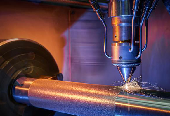
The German research institute Fraunhofer Institute for Laser Technology has developed a groundbreaking metal part coating process called Extreme High Speed Laser Material Deposition (EHLA). This innovative technique promises to revolutionize the way metal coatings are applied, offering significant improvements in efficiency, speed, and environmental impact.

How EHLA Works

EHLA involves using a laser to create a molten pool on the surface of a component. A precise amount of metal powder is then added to this pool. Unlike traditional laser deposition processes, the powder in EHLA melts completely before it is deposited on the part’s surface. This ensures a thin, uniform coating that is both durable and resource-efficient. Remarkably, EHLA introduces approximately 90% of the material into the desired area, compared to just 50% in other methods.

Extreme High Speed Laser Material Deposition

Speed and Efficiency

The standout feature of EHLA is its exceptional speed. Coating processes using EHLA can be performed at speeds 100 to 250 times faster than conventional laser material deposition techniques. This rapid application rate drastically reduces processing time, making EHLA an attractive option for high-volume production environments.

Heat Sensitivity and Versatility

One of the key advantages of EHLA is its minimal heat generation during processing. This makes it ideal for coating heat-sensitive components without causing thermal damage. Additionally, EHLA is capable of tandem coating processing, which allows for the application of multiple layers or different materials in a single operation. This versatility opens up new possibilities for advanced coatings that can enhance the performance and longevity of metal parts.

Environmental Benefits

EHLA stands out for its environmental friendliness. The process eliminates the need for chromium, a chemical commonly used in traditional coating processes that is harmful to the environment. EHLA uses no hazardous chemicals, making it a safer and more sustainable option. Moreover, the coating adheres to the substrate in a material-locking manner, preventing peeling and ensuring a long-lasting bond.

Applications and Future Prospects

Researchers are excited about the potential applications of EHLA. The process is effective in protecting metal parts from corrosion and wear, extending the life cycle of products. It is compatible with various coatings, including iron, nickel, and cobalt-based alloys, making it suitable for a wide range of industrial applications.

With its impressive speed, efficiency, and environmental benefits, EHLA presents a promising future for metal coating technologies. It offers a sustainable solution that not only enhances the performance of metal parts but also reduces resource consumption and environmental impact.

About Stanford Advanced Materials

Stanford Advanced Materials (SAM) Corporation is a global supplier of various sputtering targets such as metals, alloys, oxides, and ceramic materials. If you are interested in learning more about EHLA or our range of products, please visit our website at SAM Sputter Targets for more information.

Aluminum-Doped Zinc Oxide: Applications

Introduction

Aluminum-doped zinc oxide (AZO) is a transparent conductive oxide (TCO) that has garnered significant attention for its impressive combination of electrical conductivity and optical transparency. These properties make AZO a highly versatile material, finding applications in various fields ranging from renewable energy to advanced electronics. This article delves into the numerous applications of AZO, highlighting its critical role in modern technology. Notably, Stanford Advanced Materials is a key supplier of high-quality AZO thin-film coatings.

Solar Cells

One of the most prominent applications of AZO is in the production of solar cells. AZO serves as a transparent conductive electrode, a crucial component that allows light to reach the active layer of the solar cell while conducting the generated electrical current efficiently. Its high transparency ensures minimal loss of light, while its low resistivity facilitates effective current collection, enhancing the overall efficiency of the solar cells.

Polycrystalline Silicon Solar Cells
Ogunshile, Emmanuel. (2017). An Investigation into the Use of Hybrid Solar Power and Cloud Service Solutions for 24/7 Computing. 743-754. 10.5220/0006380007430754.

Key Points:

  • Transparent Electrode: Allows light to reach the active layer of the solar cell.
  • Efficient Current Collection: Low resistivity ensures minimal electrical losses.

Flat-Panel Displays

AZO is widely used in the manufacture of flat-panel displays, including LCDs and OLEDs. In these applications, AZO functions as a transparent conductive layer that forms part of the display’s electrode structure. Its high optical transparency ensures clear and vibrant displays, while its electrical conductivity supports the operation of the display’s pixels.

Key Points:

  • High Optical Transparency: Ensures clear and vibrant displays.
  • Conductive Layer: Supports the operation of the display’s pixels.

Touch Screens

Touch screens in smartphones, tablets, and other electronic devices rely on transparent conductive materials to detect touch inputs. AZO, with its excellent transparency and conductivity, is an ideal material for touch screen applications. It allows for precise touch detection while maintaining the screen’s clarity and responsiveness.

Key Points:

  • Precise Touch Detection: Supports accurate and responsive touch screens.
  • Maintains Screen Clarity: High transparency ensures clear display quality.

Smart Windows

Smart windows, also known as electrochromic windows, can change their transparency in response to an applied voltage. AZO is used as a transparent electrode in these windows, playing a critical role in their ability to modulate light transmission. This application is particularly valuable in energy-efficient building designs, where smart windows help regulate indoor temperature and lighting.

Key Points:

  • Modulates Light Transmission: Allows smart windows to change transparency.
  • Energy Efficiency: Contributes to temperature and lighting regulation in buildings.

Light-Emitting Diodes (LEDs)

In LED technology, AZO is used as a transparent electrode, particularly in ultraviolet and visible light LEDs. Its high conductivity and transparency enhance the efficiency of LEDs by ensuring effective current injection and minimal light absorption. This application is essential for creating bright and energy-efficient lighting solutions.

Key Points:

  • Enhances LED Efficiency: Effective current injection and minimal light absorption.
  • Bright and Energy-Efficient Lighting: Supports the development of advanced LED technologies.

Thin-Film Transistors (TFTs)

Thin-film transistors are critical components in a variety of electronic devices, including displays and sensors. AZO is employed as a channel layer or electrode material in TFTs due to its excellent electrical properties. Its use in TFTs helps improve the performance and reliability of electronic circuits.

Key Points:

  • Improves Performance: Enhances the efficiency and reliability of electronic circuits.
  • Versatile Component: Used in displays, sensors, and other electronic devices.

Photodetectors

Photodetectors, which are used to detect light and convert it into electrical signals, benefit from the use of AZO. Its high transparency and conductivity make it an ideal material for the transparent electrodes in photodetectors, improving their sensitivity and response time. This application is vital in various fields, including medical imaging, environmental monitoring, and security systems.

Key Points:

  • Improves Sensitivity: Enhances the detection capabilities of photodetectors.
  • Fast Response Time: Ensures quick and accurate light detection.

Conclusion

Aluminum-doped zinc oxide (AZO) is a versatile material with a wide range of applications in modern technology. From solar cells and flat-panel displays to touch screens and smart windows, AZO’s unique properties of high electrical conductivity and optical transparency make it an indispensable component in many advanced electronic devices. As technology continues to evolve, the role of AZO in improving efficiency, performance, and functionality in various applications is set to expand, driving innovations and enhancing the capabilities of future technologies. Stanford Advanced Materials, a leading supplier of high-quality AZO thin-film coatings, plays a crucial role in supporting these advancements.

Indium Phosphide Wafer Applications: Revolutionizing Technology Across Fields

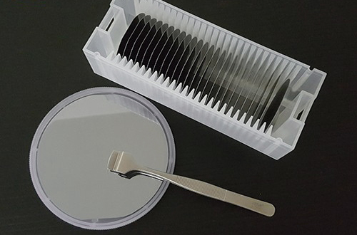
Indium phosphide (InP) wafers are at the forefront of technological innovation, serving as a foundational element in several cutting-edge applications. Known for their excellent electronic and optoelectronic properties, InP wafers are instrumental in advancing industries from automotive to telecommunications and energy. Here, we explore the diverse applications of Indium phosphide wafers, demonstrating their crucial role in modern technology.

Optoelectronic Components

Indium phosphide wafers are pivotal in the development of optoelectronic components, particularly in the realm of terahertz technology. This application is incredibly beneficial in ultra-sensitive spectroscopic analyzers used to measure the thickness of polymers and detect multilayer coatings. These capabilities are extensively utilized in the automotive industry, enhancing the precision and reliability of vehicle manufacturing processes.

High-Speed Electronics

In the domain of electronics, InP wafers are synonymous with speed and efficiency. They are essential in creating the fastest semiconductor devices currently available. Devices such as High Electron Mobility Transistors (HEMTs) and Heterostructure Bipolar Transistors (HBTs) rely on InP for their operations. The high-speed capabilities of microelectronics developed on InP make them indispensable in sectors where rapid data processing and transmission are required, such as telecommunications and advanced computing.

Photovoltaics

Indium phosphide also plays a transformative role in the energy sector, particularly in solar power technology. Photovoltaic cells made with InP substrates are among the most efficient, with performance capabilities reaching up to 46% efficiency. The key to this high efficiency is InP’s optimal bandgap combination, which allows for effective conversion of solar radiation into electrical energy. The unique lattice constant of InP is ideal for growing low bandgap materials with high crystalline quality, critical for high-performance solar cells.

Photonic Integrated Circuits

Beyond these applications, InP is also a crucial material in the manufacturing of photonic integrated circuits (PICs). These circuits integrate active laser generation, amplification, control, and detection, all on a single chip. The properties of InP make it excellent for these functions, which are essential in communication and sensing technologies. Photonic integrated circuits based on InP are fundamental in pushing the boundaries of optical communication, including fiber optics and laser technologies.

Unlocking the Terahertz Range

Indium phosphide-based components have the unique ability to unlock the terahertz zone of the electromagnetic spectrum, which lies between infrared and microwaves. This part of the spectrum is significant for its hybrid properties, combining high-frequency and high-optical qualities, which are promising for future applications in imaging, sensing, and wireless communications.

Conclusion

The versatility and superior properties of Indium phosphide wafers make them a cornerstone in multiple high-tech applications across various industries. From enhancing the efficiency of solar panels to enabling high-speed electronics and advancing optical communications, InP wafers continue to be integral to the evolution of technology. As research progresses and the potential applications of this material expand, InP may soon play a part in even more revolutionary technologies.

For high-quality InP wafer or other crystal substrates, please visit https://www.sputtertargets.net/product-category/crystal-substrates/.

Exploring the Diverse Applications of Tungsten Sputtering Targets

Tungsten sputtering targets are pivotal in numerous industrial and technological sectors, primarily due to tungsten’s outstanding properties such as high melting point, hardness, and electrical conductivity. These targets are used in various applications from electronics to decorative coatings, playing a crucial role in enhancing product performance and durability. Here’s a deeper look into the various applications of tungsten sputtering targets:

1. Semiconductor Manufacturing

In the semiconductor industry, the use of tungsten is essential for the creation of integrated circuits. Tungsten sputter targets are employed to deposit thin films that form part of the transistor structures in semiconductor devices. The metal’s excellent electrical conductivity and robustness against electromigration make it an ideal choice for metallization processes. This involves forming conductive barrier layers and contact points within semiconductor chips, which are critical for the device’s functionality and longevity.

Thin Film Transistors

2. Thin-Film Transistors in TFT-LCD Screens

Tungsten layers are crucial components in thin-film transistors (TFT) used in LCD screens. These screens rely on tungsten when high image definition, optimized contrast, and large screen formats are required. The properties of tungsten help in achieving precise control over the electronic properties of the screens, which is essential for enhancing the quality and clarity of the display.

LCD screen

3. Microelectronics

Beyond large-scale displays, tungsten targets find significant utility in the realm of microelectronics. They are used to create various layers in frequency filters such as surface acoustic wave (SAW) filters and bulk acoustic wave (BAW) filters. These components are vital in telecommunications and consumer electronics for managing signal frequencies and enhancing device performance.

4. Creation of Diffusion Barriers and Conductor Tracks

In microelectronic components, tungsten targets are used to deposit diffusion barriers made of tungsten-nitride. These barriers prevent the intermixing of different metals and maintain the integrity of the device’s architecture. Additionally, tungsten is used to form conductor tracks, which are essential for the electrical connectivity within the device.

5. Transparent Layers for OLED Displays

Reactively sputtered tungsten oxide layers are employed in the production of OLED displays. These transparent layers are critical for the display’s performance, contributing to the color purity and efficiency of the light-emitting components. The use of tungsten in such applications underscores its versatility and value in advanced display technologies.

6. Wear and Corrosion Resistant Coatings

Tungsten is extensively used for producing wear-resistant coatings for tools and machine components. These coatings significantly enhance the durability and lifespan of the tools, making them more efficient and resistant to harsh operational conditions. Similarly, tungsten’s chemical stability makes it suitable for corrosion-resistant coatings, which protect industrial equipment from environmental degradation.

7. Decorative Coatings

The robust and lustrous nature of tungsten also lends itself to decorative applications. Tungsten coatings are used to provide a durable and aesthetically appealing finish on various consumer products, combining functionality with style.

Conclusion

The applications of tungsten sputtering targets are diverse and critical across various industries. From enhancing the performance of electronic devices to providing durable solutions in harsh environments, tungsten continues to be an indispensable material in advanced manufacturing and technology development. Its unique properties not only facilitate innovation in current technologies but also pave the way for future advancements in material science and engineering.

Read more: Everything You Need to Know About Tungsten Sputter Targets

Visit our main website: https://www.sputtertargets.net/

How to Produce Metal Powders for 3D Printing?

Introduction

Metal powders are pivotal in the world of additive manufacturing, providing the raw materials necessary for 3D printing applications across aerospace, automotive, and medical industries. The choice of metal powder significantly affects the characteristics and quality of the final printed objects. Therefore, understanding the production methods of these powders is essential for ensuring they meet specific industry standards and functional requirements. This article provides a comprehensive overview of different methods used to produce metal powders, each tailored for optimal performance in various 3D printing processes. By examining the nuances of these production techniques, we aim to illuminate how each method influences the properties of metal powders, thereby guiding manufacturers in selecting the most suitable process for their particular needs in 3D printing technology.

Spherical Inconel 600 Powder
Spherical Inconel 600 Powder for 3D Printing

Atomization Method

The atomization process is one of the most prevalent methods for producing metal powders, particularly for 3D printing. This technique involves melting the metal and then dispersing it into fine droplets using a high-pressure fluid medium. As these droplets cool and solidify, they form metal powders of varying sizes, suitable for various additive manufacturing applications.

Gas Atomization: In this variant, a high-pressure gas stream, typically argon or nitrogen, is used to break the molten metal stream into fine particles. The rapid cooling involved in gas atomization helps in obtaining powders with spherical shapes and high packing density, which are ideal for 3D printing due to their excellent flow characteristics and uniformity.

Water Atomization: This method uses high-pressure water to atomize the molten metal instead of gas. Water atomization generally results in slightly irregular powder shapes and larger particle sizes compared to gas atomization. However, it is more cost-effective and can still produce powders suitable for certain types of 3D printing applications that do not require extremely high precision or surface finish.

Solid-State Reduction Method

Solid-state reduction is a pivotal method for producing metal powders, especially for metals where high purity and specific particle characteristics are required. This process involves reducing metal oxides to metals using a reducing agent at elevated temperatures in a solid-state reaction.

The process typically uses hydrogen or carbon monoxide as the reducing agent. These gases react with metal oxides, such as iron oxide or tungsten oxide, to form pure metal powders and water or carbon dioxide as byproducts. The reaction conditions, including temperature and atmosphere, are carefully controlled to optimize purity and particle size.

Materials and Conditions: Common materials produced using the solid-state reduction method include iron, tungsten, and molybdenum powders, which are pivotal in various industrial applications including magnetic materials and high-density parts. The process is conducted in batch or continuous furnaces under a controlled atmosphere to prevent oxidation and ensure uniform reduction.

Specific Metals: This method is particularly beneficial for metals that require high purity and specific morphological characteristics that influence the mechanical properties of the final product. Metals such as tungsten and molybdenum are often produced via this method due to their high melting points, which makes other methods less viable.

Electrolysis Method

The electrolysis method is another effective technique for producing metal powders, particularly suitable for metals that can be deposited from aqueous solutions. This process involves the electrochemical reduction of metal ions in a solution to form fine metal powders.

Process Description: In electrolysis, a metal salt solution acts as the electrolyte. An electrical current is passed through this solution between two electrodes, causing the metal ions to reduce and deposit on the cathode as a solid metal powder. The conditions such as current density, temperature, and electrolyte composition are critical for controlling the particle size and morphology of the powder.

Types of Metals and Applications: Metals commonly produced by electrolysis include copper, nickel, and silver. These powders are used in applications requiring high conductivity and purity, such as electrical contacts and conductive adhesives. Electrolysis is particularly favored for its ability to control the particle structure and purity, which are crucial in electrical and electronic applications.

Advantages and Limitations: One of the significant advantages of the electrolysis method is the high purity of the powders produced, as the metal ions can be selectively reduced and deposited. However, the method’s limitations include high energy consumption and the need for careful disposal or recycling of the electrolytic solutions to prevent environmental contamination.

Read more: Metal Powder Materials Used in 3D Printing

Challenges in Metal Powder Production

Producing metal powders for 3D printing presents several challenges that impact the quality and functionality of the final product. Key issues include achieving uniform particle size distribution, maintaining high purity levels, and controlling the morphology of the particles. These factors are crucial as they directly affect the flowability, packing density, and sinterability of the powders during the printing process. Additionally, contamination from the production environment or the processing equipment can significantly degrade the properties of the metal powders, requiring stringent quality control measures and advanced purification technologies to ensure that the powders meet the rigorous standards of additive manufacturing.