Preparation of Molybdenum Sputtering Targets by Powder Metallurgy

Molybdenum film has many advantages such as good electrical conductivity and thermal stability, chemical resistance, and low thermal expansion coefficient. It has been widely used in solar power generation, computer circuits, flat panel displays, storage media, and other aspects.

The magnetron sputtering technology has many advantages such as densely rented thin films, low surface roughness, good film-base bonding force, high deposition rate, low substrate temperature, and convenient deposition of thin films with high melting points. It is currently the main method for preparing molybdenum films using molybdenum sputtering targets.

Previous studies have shown that the choice of different magnetron sputtering equipment and process parameters (target current, target power, gas pressure, sputtering time, etc.) should also have a close relationship with the differences in the structure and performance of the sputtered thin films.

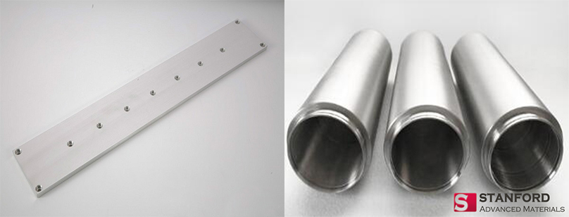
molybdenum target powder metallurgy

The electronic display industry’s technical requirements for sputtering targets mainly include indicators such as chemical purity, density, grain size and size distribution, grain orientation and orientation distribution. Recent studies have shown that the smaller the grain size of the target, the higher the sputtering rate; the more uniform the grain size distribution of the target, the easier it is to obtain a sputtered film with uniform thickness.

Since molybdenum is a high melting point (2620 ° C) metal. Powder metallurgy is the main method for preparing molybdenum targets. The process mainly includes the steps of milling, pressing, and sintering.

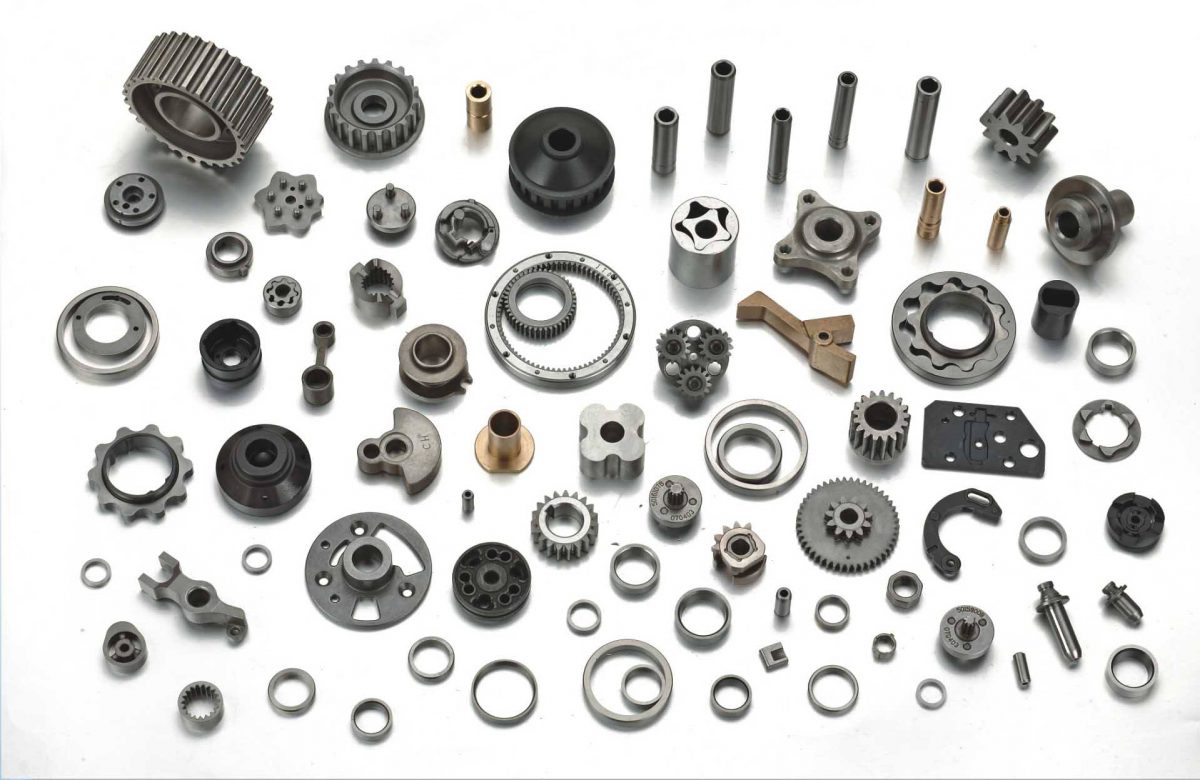
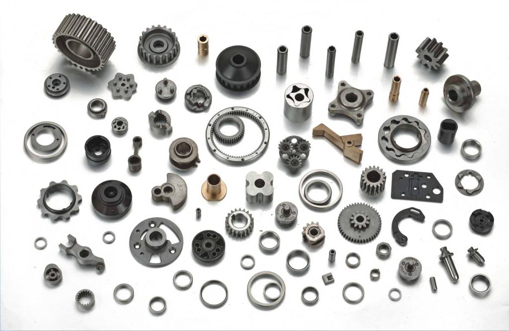
The powder metallurgy method is a technical method in which metal powders, alloy powders or mixed powders of metals and non-metals are directly made into various products through pressing, sintering and other processes. The main feature of this method is that it can produce special material products that are difficult to achieve or cannot be manufactured by conventional metallurgical methods or material processing methods, such as parts of machines made of refractory tungsten and molybdenum metals.

The main features of powder metallurgy are: the raw materials can be directly manufactured into qualified products according to the shape and size requirements of parts and components without mechanical cutting or slight cutting; suitable for mass production and high efficiency; Less waste during production and high utilization of raw materials. This method has been widely used in the automotive industry, energy industry, chemical industry, national defense industry, and aviation and aerospace industries.

For more information, please visit https://www.sputtertargets.net/.
Advantages of Sputtering Deposition and Vacuum Evaporation

For all devices, there is a need to go from semiconductor to metal. Thus we need a means to deposit metals, also called film coating. There are currently several methods for depositing metal thin film layers, and many of these techniques for metal deposition can also be used to deposit other materials.

1.) Physical Vapor Deposition (PVD)

2.) Electrochemical techniques

3.) Chemical Vapor Deposition (CVD)

This passage will talk about the advantages of two PVD methods: Sputtering and evaporation.

Sputtering Deposition

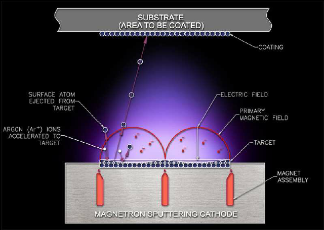
magnetron-sputtering-system
Magnetron Sputtering System

The plasma under high pressure is used to “sputter” metal atoms out of the “target”. These high-energy atoms are deposited on a wafer near the sputtering target material. Higher pressures result in better step coverage due to more random angular delivery. The excess energy of the ions also helps increase surface mobility (the movement of atoms on the surface).

Advantages: Better step coverage, less radiation damage than E-beam evaporation, easier to deposit alloys.

Disadvantages: Some plasma damage including implanted argon. Good for ohmics, not Schottky diodes.

Vacuum Evaporation

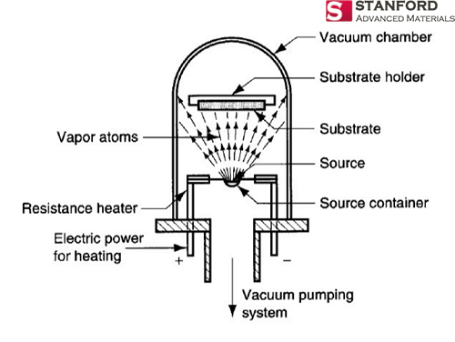
Evaporation (PVD)
Evaporation (PVD)

Evaporation is based on the concept that there exists a finite “vapor pressure” above any material. The material either sublimes (direct solid to vapor transition) or evaporates (liquid to vapor transition).

Advantages: Highest purity (Good for Schottky contacts) due to low pressures.

Disadvantages: Poor step coverage, forming alloys can be difficult, lower throughput due to low vacuum.

PVD Film Morphology

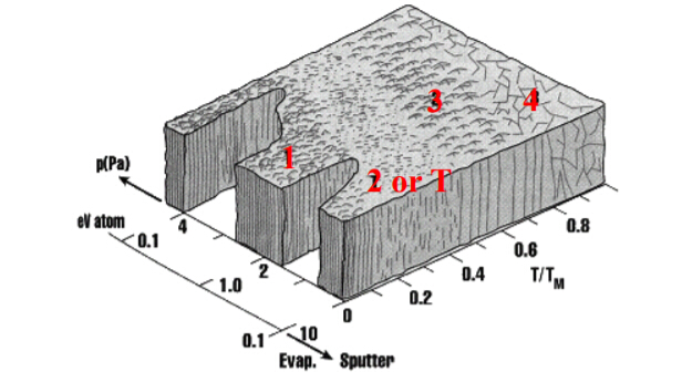
The three zone model of film deposition as proposed by Movchan and Demchishin

1.) Porous and/or Amorphous —> Results from poor surface mobility =low temperature, low ion energy (low RF power/DC bias or higher pressures=less acceleration between collisions).

2.) “T-zone”: Small grain polycrystalline, dense, smooth and high reflectance (the sweet spot for most metal processes) Results from higher surface mobility =higher temperature or ion energy

3.) Further increases in surface mobility result in columnar grains that have rough surfaces. These rough surfaces lead to poor coverage in later steps.

4.) Still further increases in surface mobility result in large (non-columnar) grains. These grains can be good for diffusion barriers (less grain boundary diffusion due to fewer grains) but pose problems for lithography due to light scatter off of large grains, and tend to be more rigid leading to more failures in electrical lines.

For more information, please visit https://www.sputtertargets.net/.
Sputter Targets for the Chip Industry

Every era has some materials to follow the mainstream trend to become the leader in the industry. Under the current situation, the development of the chip industry as a high-tech commanding point has important strategic significance, and the sputter target is a necessary raw material for the manufacture of ultra-large-scale integrated circuits. Therefore, the sputtering target material may be representative of the material emerging from this mainstream trend.

In the chip industry, which is a high-tech high point, sputter targets are essential raw materials for the manufacture of very large scale integrated circuits. Very large scale integrated circuits are those with more than 100,000 components integrated on a single chip, or more than 10,000 gates. With this technology, an electronic subsystem and even the entire electronic system can be “integrated” on one chip to complete various functions such as information collection, processing, and storage. What is repeatedly used in the manufacturing process of ultra-large-scale integrated circuits is the sputtering process belonging to physical vapor deposition (PVD) technology, which is also one of the main techniques for preparing electronic thin film materials.

The principle of the sputtering process is to utilize the ions generated by the ion source to accelerate the polymerization into a high-speed ion current in a vacuum to bombard the solid surface, and the kinetic energy exchange between the ions on the surface of the ion and the solid surface causes the atoms on the solid surface to leave the target and deposit on the substrate to form a nano/micro film.

The bombarded solid is the sputtering target, which is simply like a printing mold. The quality of the target plays a crucial role in the performance of the film, which directly determines the quality and performance of downstream semiconductor chips, flat panel displays, solar cells and other electronic devices or optical components. Therefore, the sputter target is the key raw material in the whole process.

Sputtering targets can be classified according to their chemical composition, geometry and field of application. Targets with different compositions (aluminum, copper, stainless steel, titanium, nickel targets, etc.) can be divided into different film systems (superhard, wear-resistant, anti-corrosion alloy films, etc.); if divided according to their application fields, they can be divided into It is recording medium targets, semiconductor targets, display film targets, superconducting targets, and optical targets.

The target production process includes two processes of “material purification” and “target preparation”. During the purification process, it is necessary to ensure the reduction of impurity content in the target, and the preparation process needs to ensure the surface level of the sputter coater target.

Sputtering targets for high-end applications have very high technical thresholds and are very complex to prepare. First of all, it is necessary to carry out process design according to performance requirements, and then carry out repeated plastic deformation, heat treatment, precise control of grain, crystal orientation and other indicators, and then through welding, machining, cleaning and drying, vacuum packaging and other processes.

For more information, please visit https://www.sputtertargets.net/.
What are the Uses of Metal Sputtering Targets?

What is the “target”?

The target refers to the target material. They can be used in high-energy laser weapons; different power densities, different output waveforms, and different wavelengths of lasers can have different killing effects when interacting with different targets. Another major use for them is for sputtering in physical film coating.

What is the “sputtering target”?

Magnetron sputtering coating is a new type of physical vapor deposition method, and its advantages in many aspects are quite obvious compared with the earlier evaporation coating method. As a relatively mature technology that has been developed, magnetron sputtering has been applied in many fields. Sputtering targets serve as source materials in magnetron sputtering coatings.

sputtering target in lcd

What are the application areas?

1: Microelectronics field

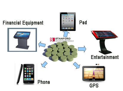
2: Target for flat panel display

3: Targets for storage technology

Sputtering materials are mainly used in electronics and information industries, such as integrated circuits, information storage, liquid crystal displays, laser memories, electronic control devices, etc.; they can also be used in the field of glass coating; they can also be applied to wear-resistant materials, high temperature corrosion resistance, high-grade decorative products and other industries.

The technological development trend of target materials is closely related to the development trend of thin-film technology in the downstream application industry. As technology in the application industry improves on film products or components, target technology should also change. In recent years, flat panel displays (FPDs) have largely replaced the market for computer monitors and televisions, which are mainly cathode ray tubes (CRTs), and will greatly increase the technical and market demand for ITO targets.

Stanford Advanced Materials (SAM) Corporation is a global supplier of various sputtering targets such as metals, alloys, oxides, ceramic materials. For more information, please visit https://www.sputtertargets.net/.
Applications of High Purity Copper Sputtering Target

The copper sputtering target is a coating material made of metallic copper, which is suitable for DC bipolar sputtering, three-pole sputtering, four-stage sputtering, radio frequency sputtering, counter target sputtering, ion beam sputtering, and magnetron sputtering, etc. It can be applied to manufacture reflective films, conductive films, semiconductor films, capacitor films, decorative films, protective films, integrated circuits, displays, and etc. Compared with other precious metal sputtering targets, the price of copper targets is lower, so the copper target is the preferred target material under the premise of satisfying the function of the film layer.

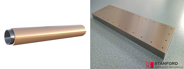
Copper sputter targets are divided into the planar copper target and rotary copper target. The former is sheet-shaped, with round, square, and the like; the latter is tubular, and the utilization efficiency is high.

planar and rotory copper sputtering target

High-purity copper sputter targets are mainly used in electronics and information industries, such as integrated circuits, information storage, liquid crystal displays, laser memories, electronic control devices, etc.; they can be applied to the field of glass coating; they can also be applied to wear-resistant materials, high-temperature corrosion resistance, high-end decorative supplies and other industries.

Information storage industry: With the continuous development of information and computer technology, the demand for recording media in the world market is increasing, and the corresponding target media for recording media is also expanding. Related products include hard disks, magnetic heads, and optical disks. (CD-ROM, CD-R, DVD-R, etc.), a magneto-optical phase-change optical disc (MO, CD-RW, DVD-RAM).

Integrated circuit industry: In the field of semiconductor applications, sputtering targets are one of the main components of the world target market. They are mainly used for electrode interconnect film, barrier film, contact film, optical disk mask, capacitor electrode film, and resistive film, etc.

Flat-panel display industry: Flat panel displays include liquid crystal displays (LCDs), plasma displays (PDPs), and the like. At present, LCD is the main market in the flat panel display market, and its market share exceeds 85%. LCD is considered to be the most promising flat display device and is widely used in notebook monitors, desktop monitors and high definition televisions. The manufacturing process of the LCD is complicated, in which the reflective layer, the transparent electrode, the emitter and the cathode are all formed by a sputtering method, and therefore, the sputtering target plays an important role in the manufacture of LCD.

For more information, please visit https://www.sputtertargets.net/.

Introduction to Aluminum, Aluminum Alloy and Aluminum Sputtering Target

Aluminum is a light metal with low density (2.79/cm3), good strength and excellent plasticity. As for aluminum alloy, the strength of super-hard aluminum alloy can reach 600Mpa, and the tensile strength of ordinary hard aluminum alloy can reach 200-450Mpa, which is much higher than steel in steel. Therefore, aluminum and aluminum alloy are widely used in machinery manufacturing.

The conductivity of aluminum is second only to silver and copper, so aluminum is used in the manufacture of various conductors. Aluminum also has a good thermal conductivity that can be used as a variety of heat dissipating materials. Besides, aluminum has good corrosion resistance and excellent plasticity, and is suitable for various pressure processing.

Aluminum alloy

Aluminum alloy can be divided into the deformed aluminum alloy and the cast aluminum alloy according to the processing method.

The deformed aluminum alloy can be further divided into a non-heat treatable reinforced aluminum alloy and a heat treatable reinforced aluminum alloy. Non-heat-treated reinforced aluminum alloy cannot improve the mechanical properties by heat treatment, and can only be strengthened by cold working deformation. It mainly includes high-purity aluminum, industrial high-purity aluminum, industrial pure aluminum and rust-proof aluminum. The heat-treatable reinforced aluminum alloy can be improved in mechanical properties by heat treatment such as quenching and aging, and can be classified into hard aluminum, wrought aluminum, super-hard aluminum, and special aluminum alloy. The aluminum alloy can be heat treated to obtain good mechanical properties, physical properties and corrosion resistance.

Cast aluminum alloy can be divided into aluminum-silicon alloy, aluminum-copper alloy, aluminum-magnesium alloy and aluminum-zinc alloy according to chemical composition. Cast aluminum alloy is classified into four types according to the main elements other than aluminum in the composition: silicon, copper, magnesium and zinc.

Pure aluminum products

Pure aluminum products are divided into two categories: smelting and pressure processing. The former is represented by chemical composition Al, and the latter is represented by LG (aluminum, industrial). The aluminum sputtering target is a kind of pure aluminum product.

Pressure processing aluminum alloy

Aluminum alloy pressure processing products are divided into seven categories: rustproof (LF), hard (LY), forged (LD), superhard (LC), coated (LB), special (LT) and brazed (LQ). The state of the commonly used aluminum alloy material is three types of annealing (M igniter), hardening (Y), and hot rolling (R).

Aluminum sputtering target

The aluminum sputtering target is one of the sputtering targets used in the vacuum coating industry, and is therefore called aluminum sputtering target. The aluminum target is obtained after a series of processing of high-purity aluminum. It is available in a specific size and shape, which is mounted on a vacuum coater to form a film on the surface of the substrate by sputtering.

Please visit https://www.sputtertargets.net/ for more information.

Application of Indium Tin Oxide in Anti-Reflection Film Design

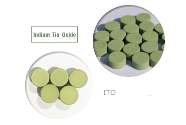
The indium tin oxide (ITO) transparent conductive film belongs to an N-type oxygen-deficient semiconductor material. It has low absorption of visible light and has high visible light transmittance, excellent infrared reflection performance and microwave attenuation performance in the mid-far infrared range. ITO transparent conductive film has become an important optical component in the field of optoelectronic devices due to its excellent photoelectric performance.

indium tin oxide evaporation pellets

ITO materials have long been used as transparent conductive films in the form of single-layer films, but their average transmittance in the visible portion is very low, generally less than 90%, and the reflectance is high, affecting its display and electromagnetic shielding applications. If the transmittance in the visible light region is improved, the application of the ITO transparent conductive film will be more extensive.

The ITO film is usually made of the indium tin oxide sputtering target and the indium tin oxide evaporation material. The use of the ITO film as one of the antireflection film systems can greatly increase the transmittance of the transparent conductive film in the visible light portion, and solves the problem that the transparent conductive film is generally low in visible light transmittance. A multilayer anti-reflection film containing TTO material was prepared by a low-pressure reactive ion plating method, and a transparent conductive film having an average visible light transmittance of 95.83%, a maximum transmittance of 97.26%, and a sheet resistance of 13.2 to 24.6 Ω was obtained. The anti-reflection film largely alleviates the contradiction between the conductivity and the transparency of the transparent conductive film, and the ITO transparent conductive film has more useful practical value and application prospect in the field of application.

indium tin oxide uses

For more information, please visit https://www.sputtertargets.net/.
Rotatable Sputtering Targets Merits and Weakness

Sputtering is a high-speed process where superfast ions hit a sputtering target and dislodge minuscule particles that in turn coat a thin film on substrates like architectural glass, LED televisions and computer displays.

Rotatable sputtering target, or rotatory target, is a commonly used target shape in magnetron sputtering. It is generally cylindrical, with a stationary magnet inside, and a slow magnetic field, which allows the sputtering rate to be uniform and the target utilization rate to be high. Rotating targets are commonly used for coating solar cells, architectural glass, automotive glass, semiconductors, and flat-panel TVs.

The main advantage of the rotatable target is the high utilization of the target, which means that the rotating target can solve the problem of low utilization of the planar target.

Rotatory Copper (Cu) Sputtering Target

For a planar sputtering target, the target utilization of the normal cathode can reach 25%, and the special design of the magnet bypass with the target back can increase the target utilization to about 40%. Despite this, the utilization of planar targets is still not high. However, the utilization of cylindrical rotating targets is typically in the range of 75% to 90%, much higher than planar targets. However, when the rotating target is used for large-area coating, the uniformity of the surface of the film layer is poor and it is difficult to meet the requirements, which is the biggest disadvantage of the rotating target.

Materials Planar Rotatory
Metal Planar molybdenum target, planar copper target, planar titanium target, planar tungsten target, planar zirconia target


Rotatory molybdenum target, rotatory copper target, rotatory titanium target, rotatory tungsten target, rotatory zirconia target


Oxides Planar SiO2 Sputtering Target Rotatory ATO Sputtering Target, rotary Nb2Ox sputtering target, rotatory TiOx sputtering target, rotatory Al2O3 sputtering target
Alloy Planar Cr-Ta sputtering target, planar Ti-Al-Si sputtering target SnO2-Sb2O3 rotatory sputtering target

For more information, please visit https://www.sputtertargets.net/.

Sputtering Target Materials for Vacuum Thin Film Coating

The sputtering target is a key required material for vacuum film coating. It refers to a material that can ionize the surface by the current-binding magnetic field.

Almost all sputter coating equipment uses a powerful magnet to spiral the electrons to accelerate the ionization of the argon around the target, resulting in an increased likelihood of collision between the target and the argon ions, thereby increasing the sputtering rate.

Typically, most metal plating uses DC sputtering, while non-conductive ceramic materials use RF sputtering. The basic principle is that argon (Ar) ions are struck against the target surface by glow discharge in a vacuum, and cations in the plasma are accelerated as a sputter material to the surface of the negative electrode. The impact will cause the material of the target to fly out and deposit on the substrate to form a film.

Generally, the sputter coating process has several features:

(1)Many materials can be deposited into thin film materials by sputtering, including metals, alloys, insulators, and the like.

(2)Under appropriate conditions, different component target materials can be made into films of the same material.

(3)Oxides or other compounds of the target substance and gas molecules can be prepared by adding oxygen or other reactive gas to the discharge atmosphere.

(4)Highly accurate film can be obtained by controlling the magnitude of the input current and the length of the sputtering time.

(5)For large-area coatings, sputter deposition is definitely superior to other coating processes.

(6)In the vacuum vessel, the sputtered particles are not affected by gravity, and the positions of the target and the substrate can be freely aligned.

(7)The bond strength between the sputter-coated substrate and the film is 10 times or more the adhesive strength of a general evaporated deposited film. Furthermore, since the sputtered particles have high energy, the surface of the film is continuously diffused to obtain a hard and dense film. At the same time, high energy allows the substrate to obtain a crystalline film at a lower temperature.

(8)The nucleation density at the initial stage of film formation is high, and an extremely thin continuous film of 10 nm or less can be produced.

(9)Sputtering targets have a long service life and can be continuously produced over a long period of time.

(10)The sputtering target can be made into various shapes. By special design of the shape of the target, the sputtering process can be better controlled and the sputtering efficiency can be most effectively improved.

For more information, please visit https://www.sputtertargets.net/.
Pros and Cons of Ion Beam Sputtering

Advantage

1 Ion beam sputtering relies on momentum exchange to make atoms and molecules of solid materials enter the gas phase. The average energy generated by sputtering is 10 eV, which is about 100 times higher than that of vacuum evaporation. After deposited on the surface of the substrate, these particles still have enough kinetic energy to migrate on the surface of the substrate, so that the film has good quality and is firmly bonded to the substrate.

2 Any material can be coated by ion beam sputtering, and even a high-melting material can be sputtered. For alloys and compound materials, it is easy to form a film having the same ratio as the composition of the sputtering target, and thus sputter coating is widely used.

3 The incident ions of the ion beam sputter coating are generally obtained by a gas discharge method, and the working pressure is between 10-2 Pa and 10 Pa. Sputtered ions often collide with gas molecules in the vacuum chamber before flying to the substrate, so the direction of motion randomly deviates from the original direction. Sputtering is generally ejected from a larger sputter target surface area and is, therefore, more uniform than that obtained by vacuum coating. For coating parts with grooves, steps, etc., the sputter coating can reduce the difference in film thickness caused by the cathode effect to a negligible extent. However, sputtering at higher pressures will result in more gas molecules in the film.

ion beam sputtering deposition

4 Sputtering can precisely focus and scan the ion beam, change the target material and substrate material while maintaining the characteristics of the ion beam, and independently control the ion beam energy and current. Since the energy of the ion beam, the beam size and the beam direction can be precisely controlled, and the sputtered atoms can directly deposit the film without collision, the ion beam sputtering method is suitable as a research method for thin film deposition.

Disadvantage

The main disadvantage of ion beam sputtering is that the target area of the bombardment is too small and the deposition rate is generally low. What’s worse, ion beam sputter deposition is also not suitable for depositing a large-area film of uniform thickness. And the sputtering device is too complicated, and the equipment operating cost is high.

For high purity sputtering target inquiry, please visit Stanford Advanced Materials.