
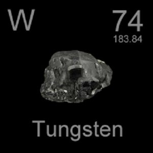
The history of tungsten dates back to the 17th century. At that time, miners in the Erzgebirge Mountains of Saxony, Germany, noticed that some of the ore would interfere with the reduction of cassiterite and produce slag. The miners gave the mines some German nicknames: “wolfert” and “wolfrahm”.
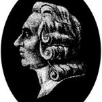
In 1758, the Swedish chemist and mineralogist Axel Fredrik Cronstedt discovered a mineral called “tungsten”, which means “heavy stone” in Swedish. He was convinced that this mineral contained an element that had not yet been discovered.
Continue reading “Discovery and development of tungsten | History of Tungsten”


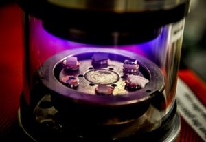 First, let’s take a look at the definition of these two words. The vacuum evaporation is carried out by means of resistance heating, electron beam or laser bombardment in an environment with a vacuum of not less than 10-2 Pa, and the