What are the advantages of carbon fiber composite materials used in aeroplanes?

Carbon fiber is a kind of special fiber mainly composed of carbon element and generally contains more than 90% carbon. Carbon fiber has the characteristics of high-temperature resistance, friction resistance, electrical conductivity, thermal conductivity, and corrosion resistance to general carbon materials. However, unlike ordinary carbon materials, its shape has significant anisotropy, and it shows strong strength along the fiber axis.

With its own unique advantages, carbon fiber reinforced composites have also been widely used in the aircraft manufacturing industry. Especially for smaller airplanes, carbon fiber composites are the best choice.

As a kind of carbon fiber, carbon fiber composite material has a wide range of applications in many fields due to its characteristics of high strength, lightweight, stable chemical properties, high-temperature resistance, and strong durability. Applying it to the fuselage and wings of an airplane can reduce the weight of the airplane by about 40%, and its crawling ability can be increased by 1.8 times compared with the airplane of ordinary materials.

Compared with military and civil aircraft, model aircraft are smaller in size, shorter in-flight operation time, and the working environment is relatively better. Applying carbon fiber composite materials to model aircraft can increase their service life, so they can be applied to the harsh environments.

aircraft concord

The application of carbon fiber composite materials to airplane aircraft can not only reduce the mass of the airplane but also increase the strength tolerance range of the airplane aircraft to a certain extent. The fuselage and propeller made of carbon fiber composite materials reduce the weight of the airplane while increasing its strength, thereby reducing its volume.

With the continuous development of the aerospace industry, the demand for carbon fiber composites is increasing. At the same time, people have put forward higher requirements for the quality of carbon fiber composite materials, which in a certain sense promotes the development of carbon fiber composite materials in the direction of multifunctionality, low cost and high performance.

Compared with glass fiber, the application cost of carbon fiber is also relatively high, and it is more difficult to promote and use it in a wide range. From the current situation, the price of carbon fiber materials has not only declined, but also shown an upward trend. To solve this problem, new processes must be studied to reduce the cost of carbon fiber composites.

Carbon fiber materials can also be made into the carbon sputtering target for aviation coatings. Stanford Advanced Materials provides high-quality sputtering targets and evaporation materials. Please visit https://www.sputtertargets.net for more information.

Silicon Wafer: 4 Types of Wet Cleaning Method

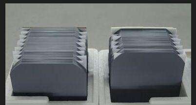
After the silicon wafer is processed by different processes such as slicing, chamfering, grinding, surface treatment, polishing, and epitaxy, the surface has been seriously stained. The purpose of cleaning the Si wafer is to remove particles, metal ions and organic substances on the surface of the silicon wafer.

Semiconductor-Silicon-Wafers

Wet cleaning uses chemical solvents with strong corrosive and oxidizing properties, such as H2SO4, H2O2, DHF, NH3•H2O, etc. The impurity particles on the surface of the silicon wafer react with the solvent to form soluble substances and gases. In order to improve the cleaning effect, it is possible to use mega-acoustic, heating, vacuum and other technical means, and finally use ultra-pure water to clean the surface of the silicon wafer to obtain a silicon wafer that meets the cleanliness requirements.

There are several methods for wet cleaning the silicon semiconductor wafer:

RCA Cleaning for Silicon Wafer

Kern et al. proposed the RCA cleaning method in 1965. According to the SPM, DHF, SC-1, and SC-2 sequences, the RCA cleaning method basically satisfies the requirements of most wafer cleanliness. Cleaning the silicon wafers by this method not only improves the cleaning efficiency, reduces the cost, saves time, obtains excellent surface cleanliness, but also improves the electrochemical performance of the Si wafer.

Ultrasonic Cleaning for Silicon Wafer

Ultrasonic cleaning is a cleaning method widely used in the semiconductor industry. The method has the advantages of good cleaning effect, simple operation, and can be removed for complicated devices and containers; but the method also has the disadvantages of high noise and easy breakage of the transducer.

This method can effectively remove organic, particulate, and metal ion impurities on the surface of the silicon wafer by utilizing the mechanical action of high-frequency sound waves, the cavitation effect of the solution, and the complexation reaction of chemical reagents. Using a similar method, BongKyun et al. used a 0.83 MHz megasonic wave to clean the silicon wafer, which is more excellent and can remove particulate impurities below 0.3 μm.

Silicon Wafer Wet Cleaning

Double Flow Spray for Silicon Wafer

The dual-flow atomizing nozzle cleans the silicon wafer by using a nozzle to scan the silicon wafer back and forth with the rotating arm, and the silicon wafer rotates clockwise. The dual-flow nozzle uses a high-pressure, high-speed jet of gas to impinge a vulgar flow of liquid, destroying the surface tension of the liquid and the van der Waals bond and hydrogen bond between the liquid molecules, causing the liquid to atomize and become nanometer-sized droplets, which are ejected at high speed through the nozzle under the action of high pressure air.

Ozone Microbubble Method for Silicon Wafer

The high activity and strong oxidizing properties of ozone can remove organic and particulate impurities on the surface of the Si wafers. Ozone is dissolved in water to form a highly reactive OH group, and the OH group chemically reacts with the organic substance to remove organic impurities on the surface of the silicon semiconductor wafer. At the same time, the surface of the silicon product is covered with an atomic-level smooth oxide film, which effectively isolates the re-adsorption of impurities.

This method has an excellent cleaning effect, basically removes organic and particulate impurities, and meets the requirements of general silicon wafer cleanliness. At the same time, ozone microbubble cleaning produces less polluting waste and high cleaning efficiency, and can be used for cleaning large-scale circuits, silicon wafers and LEDs.

For more information, please visit https://www.sputtertargets.net/.

Sputter Targets for the Chip Industry

Every era has some materials to follow the mainstream trend to become the leader in the industry. Under the current situation, the development of the chip industry as a high-tech commanding point has important strategic significance, and the sputter target is a necessary raw material for the manufacture of ultra-large-scale integrated circuits. Therefore, the sputtering target material may be representative of the material emerging from this mainstream trend.

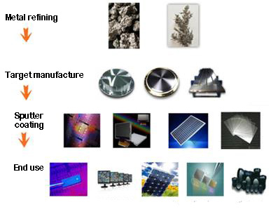
In the chip industry, which is a high-tech high point, sputter targets are essential raw materials for the manufacture of very large scale integrated circuits. Very large scale integrated circuits are those with more than 100,000 components integrated on a single chip, or more than 10,000 gates. With this technology, an electronic subsystem and even the entire electronic system can be “integrated” on one chip to complete various functions such as information collection, processing, and storage. What is repeatedly used in the manufacturing process of ultra-large-scale integrated circuits is the sputtering process belonging to physical vapor deposition (PVD) technology, which is also one of the main techniques for preparing electronic thin film materials.

The principle of the sputtering process is to utilize the ions generated by the ion source to accelerate the polymerization into a high-speed ion current in a vacuum to bombard the solid surface, and the kinetic energy exchange between the ions on the surface of the ion and the solid surface causes the atoms on the solid surface to leave the target and deposit on the substrate to form a nano/micro film.

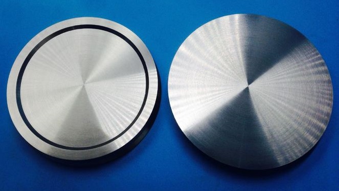
The bombarded solid is the sputtering target, which is simply like a printing mold. The quality of the target plays a crucial role in the performance of the film, which directly determines the quality and performance of downstream semiconductor chips, flat panel displays, solar cells and other electronic devices or optical components. Therefore, the sputter target is the key raw material in the whole process.

Sputtering targets can be classified according to their chemical composition, geometry and field of application. Targets with different compositions (aluminum, copper, stainless steel, titanium, nickel targets, etc.) can be divided into different film systems (superhard, wear-resistant, anti-corrosion alloy films, etc.); if divided according to their application fields, they can be divided into It is recording medium targets, semiconductor targets, display film targets, superconducting targets, and optical targets.

The target production process includes two processes of “material purification” and “target preparation”. During the purification process, it is necessary to ensure the reduction of impurity content in the target, and the preparation process needs to ensure the surface level of the sputter coater target.

Sputtering targets for high-end applications have very high technical thresholds and are very complex to prepare. First of all, it is necessary to carry out process design according to performance requirements, and then carry out repeated plastic deformation, heat treatment, precise control of grain, crystal orientation and other indicators, and then through welding, machining, cleaning and drying, vacuum packaging and other processes.

For more information, please visit https://www.sputtertargets.net/.

What are the Uses of Metal Sputtering Targets?

What is the “target”?

The target refers to the target material. They can be used in high-energy laser weapons; different power densities, different output waveforms, and different wavelengths of lasers can have different killing effects when interacting with different targets. Another major use for them is for sputtering in physical film coating.

What is the “sputtering target”?

Magnetron sputtering coating is a new type of physical vapor deposition method, and its advantages in many aspects are quite obvious compared with the earlier evaporation coating method. As a relatively mature technology that has been developed, magnetron sputtering has been applied in many fields. Sputtering targets serve as source materials in magnetron sputtering coatings.

sputtering target in lcd

What are the application areas?

1: Microelectronics field

2: Target for flat panel display

3: Targets for storage technology

Sputtering materials are mainly used in electronics and information industries, such as integrated circuits, information storage, liquid crystal displays, laser memories, electronic control devices, etc.; they can also be used in the field of glass coating; they can also be applied to wear-resistant materials, high temperature corrosion resistance, high-grade decorative products and other industries.

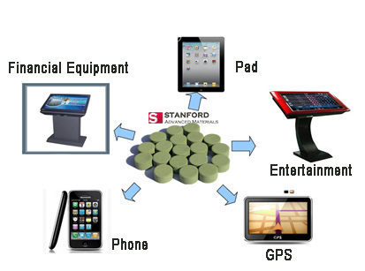
The technological development trend of target materials is closely related to the development trend of thin-film technology in the downstream application industry. As technology in the application industry improves on film products or components, target technology should also change. In recent years, flat panel displays (FPDs) have largely replaced the market for computer monitors and televisions, which are mainly cathode ray tubes (CRTs), and will greatly increase the technical and market demand for ITO targets.

Stanford Advanced Materials (SAM) Corporation is a global supplier of various sputtering targets such as metals, alloys, oxides, ceramic materials. For more information, please visit https://www.sputtertargets.net/.

Applications of High Purity Copper Sputtering Target

The copper sputtering target is a coating material made of metallic copper, which is suitable for DC bipolar sputtering, three-pole sputtering, four-stage sputtering, radio frequency sputtering, counter target sputtering, ion beam sputtering, and magnetron sputtering, etc. It can be applied to manufacture reflective films, conductive films, semiconductor films, capacitor films, decorative films, protective films, integrated circuits, displays, and etc. Compared with other precious metal sputtering targets, the price of copper targets is lower, so the copper target is the preferred target material under the premise of satisfying the function of the film layer.

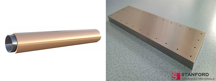
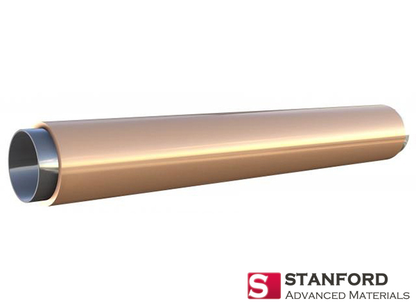
Copper sputter targets are divided into the planar copper target and rotary copper target. The former is sheet-shaped, with round, square, and the like; the latter is tubular, and the utilization efficiency is high.

planar and rotory copper sputtering target

High-purity copper sputter targets are mainly used in electronics and information industries, such as integrated circuits, information storage, liquid crystal displays, laser memories, electronic control devices, etc.; they can be applied to the field of glass coating; they can also be applied to wear-resistant materials, high-temperature corrosion resistance, high-end decorative supplies and other industries.

Information storage industry: With the continuous development of information and computer technology, the demand for recording media in the world market is increasing, and the corresponding target media for recording media is also expanding. Related products include hard disks, magnetic heads, and optical disks. (CD-ROM, CD-R, DVD-R, etc.), a magneto-optical phase-change optical disc (MO, CD-RW, DVD-RAM).

Integrated circuit industry: In the field of semiconductor applications, sputtering targets are one of the main components of the world target market. They are mainly used for electrode interconnect film, barrier film, contact film, optical disk mask, capacitor electrode film, and resistive film, etc.

Flat-panel display industry: Flat panel displays include liquid crystal displays (LCDs), plasma displays (PDPs), and the like. At present, LCD is the main market in the flat panel display market, and its market share exceeds 85%. LCD is considered to be the most promising flat display device and is widely used in notebook monitors, desktop monitors and high definition televisions. The manufacturing process of the LCD is complicated, in which the reflective layer, the transparent electrode, the emitter and the cathode are all formed by a sputtering method, and therefore, the sputtering target plays an important role in the manufacture of LCD.

For more information, please visit https://www.sputtertargets.net/.

Boron Nitride Crucible Use Guide

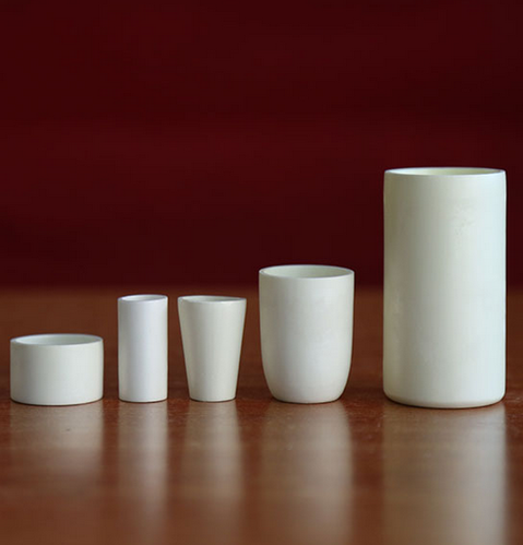
Boron nitride crucible is used at a temperature of approximately 1800 degrees under vacuum and at a temperature of approximately 2100 degrees under atmospheric protection, making it ideal for ultra-high temperature forging.

BN crucible is best used in the nitrogen or argon atmosphere and has the longest life in that environment. The thermal resistance of boron nitride crucible is good. Even if the temperature suddenly becomes cold when it is used at 1500 degrees, it will not crack; after holding it for 20 minutes in a 1000 degree furnace, take it out and blown and quenched it continuously for hundreds of time, it won’t crack, either.

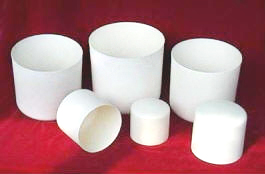
bn crucible

Precautions for use

1 When boron nitride is used in air, the temperature should not exceed 1000 degrees; if the temperature exceeds 1000 degrees, the contact surface of boron nitride and oxygen will oxidize and peel off.

2 Boron nitride is easy to absorb moisture, so BN crucible can not be stored in wet areas, can not be washed, but can be directly wiped with sandpaper or scrubbed with alcohol.

3 Applications of boron nitride

[Available materials]

  1. Ferrous metal: iron, copper, aluminum, nickel, magnesium, bismuth, zinc, etc., alloy FE-CO-NI-SI CO-ZR-NB
  2. Does not react with water or acid at normal temperature. Slowly hydrolyze with water to form boric acid and ammonia
  3. Rare earth, nitride

bn crucible-2

[Unavailable materials]

  1. Antimony trioxide, chromium oxide pentoxide, molybdenum trioxide, arsenic trioxide, titanium carbide, etc.
  2. The high-lead glass glaze melts in the air at 800-950 °C, but it does not react under the protection of nitrogen or inert gas. 3. Boron phosphate erodes boron nitride in 1400 ° nitrogen, and reacts with hot concentrated or molten alkali and hot chlorine.

For more information about evaporation e-beam source used crucibles, please visit https://www.sputtertargets.net/e-beam-source-used-crucibles.html.

Application of Indium Tin Oxide in Anti-Reflection Film Design

The indium tin oxide (ITO) transparent conductive film belongs to an N-type oxygen-deficient semiconductor material. It has low absorption of visible light and has high visible light transmittance, excellent infrared reflection performance and microwave attenuation performance in the mid-far infrared range. ITO transparent conductive film has become an important optical component in the field of optoelectronic devices due to its excellent photoelectric performance.

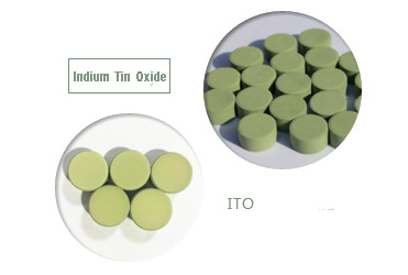
indium tin oxide evaporation pellets

ITO materials have long been used as transparent conductive films in the form of single-layer films, but their average transmittance in the visible portion is very low, generally less than 90%, and the reflectance is high, affecting its display and electromagnetic shielding applications. If the transmittance in the visible light region is improved, the application of the ITO transparent conductive film will be more extensive.

The ITO film is usually made of the indium tin oxide sputtering target and the indium tin oxide evaporation material. The use of the ITO film as one of the antireflection film systems can greatly increase the transmittance of the transparent conductive film in the visible light portion, and solves the problem that the transparent conductive film is generally low in visible light transmittance. A multilayer anti-reflection film containing TTO material was prepared by a low-pressure reactive ion plating method, and a transparent conductive film having an average visible light transmittance of 95.83%, a maximum transmittance of 97.26%, and a sheet resistance of 13.2 to 24.6 Ω was obtained. The anti-reflection film largely alleviates the contradiction between the conductivity and the transparency of the transparent conductive film, and the ITO transparent conductive film has more useful practical value and application prospect in the field of application.

indium tin oxide uses

For more information, please visit https://www.sputtertargets.net/.

Rotatable Sputtering Targets Merits and Weakness

Sputtering is a high-speed process where superfast ions hit a sputtering target and dislodge minuscule particles that in turn coat a thin film on substrates like architectural glass, LED televisions and computer displays.

Rotatable sputtering target, or rotatory target, is a commonly used target shape in magnetron sputtering. It is generally cylindrical, with a stationary magnet inside, and a slow magnetic field, which allows the sputtering rate to be uniform and the target utilization rate to be high. Rotating targets are commonly used for coating solar cells, architectural glass, automotive glass, semiconductors, and flat-panel TVs.

The main advantage of the rotatable target is the high utilization of the target, which means that the rotating target can solve the problem of low utilization of the planar target.

Rotatory Copper (Cu) Sputtering Target

For a planar sputtering target, the target utilization of the normal cathode can reach 25%, and the special design of the magnet bypass with the target back can increase the target utilization to about 40%. Despite this, the utilization of planar targets is still not high. However, the utilization of cylindrical rotating targets is typically in the range of 75% to 90%, much higher than planar targets. However, when the rotating target is used for large-area coating, the uniformity of the surface of the film layer is poor and it is difficult to meet the requirements, which is the biggest disadvantage of the rotating target.

Materials Planar Rotatory
Metal Planar molybdenum target, planar copper target, planar titanium target, planar tungsten target, planar zirconia target


Rotatory molybdenum target, rotatory copper target, rotatory titanium target, rotatory tungsten target, rotatory zirconia target


Oxides Planar SiO2 Sputtering Target Rotatory ATO Sputtering Target, rotary Nb2Ox sputtering target, rotatory TiOx sputtering target, rotatory Al2O3 sputtering target
Alloy Planar Cr-Ta sputtering target, planar Ti-Al-Si sputtering target SnO2-Sb2O3 rotatory sputtering target

For more information, please visit https://www.sputtertargets.net/.

History and Development of Copper

Sorry for that we have not updated the “Metal History” column for a long time. For previous posts of this column, please search the keyword “history”. Today, let us unveil the history of copper.

Copper is one of the earliest metals discovered by mankind and the first metal that humans began to use. Copper beads made of natural copper excavated by archaeologists in northern Iraq are supposed to have been more than 10,000 years old. Methods for refining copper from its ores were discovered around 5000BC and a 1000 or so years later it was being used in pottery in North Africa.

Part of the reason for it being used so early is simply that it is relatively easy to shape. However, it is somewhat too soft for many tools and around 5000 years ago it was discovered that when copper is mixed with other metals the resulting alloys are harder than the copper itself. As examples, brass is a mixture of copper and zinc while bronze is a mixture of copper and tin. For many centuries, bronze reigned supreme, being used for plows, tools of all kinds, weapons, armor, and decorative objects.

Mesopotamia, circa 4500 BC

Pure Metal is ineffective as a weapon and tool because of its softness. But early metallurgy experimentation by the Mesopotamians resulted in a solution to this problem: bronze, an alloy of copper and tin, was not only harder but also could be treated by forging (shaping and hardening through hammering) and casting (poured and molded as a liquid).

Mesopotamia copper

The ability to extract copper from ore bodies has been well developed. In today’s Armenia, bronze and copper alloy tools, including chisels, razors, harpoons, arrows and spearheads, have been traced back to the third millennium BC. A chemical analysis of bronze from the region indicates that common alloys of the time contained approximately 87 percent copper, 10 to 11 percent tin, and small amounts of iron, nickel, lead, arsenic, and antimony.

Egypt, circa 3500 BC

The use of copper in Egypt developed almost at the same time as Mesopotamia. The copper pipe used to transport water was used in the King Sa’Hu-Re temple in Abusir, 2750 BC. These tubes are made of thin copper plate with a diameter of 2.95 inches (75 mm) and a pipe length of nearly 328 feet (100 m). The Egyptians also used copper and bronze as mirrors, razors, utensils, weights and balances, as well as obelisks and ornaments on temples. According to biblical references, the Egyptians used a large number of bronze pillars on the porch of the Solomon Palace in Jerusalem (circa 9th century BC), which were 6 feet (1.83 meters) in diameter and 25 feet (7.62 meters) high.

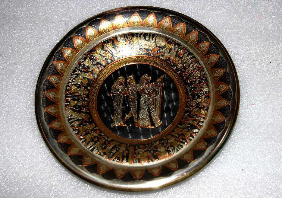
Egypt copper

China, circa 2800 BC

By the year 2000 BC, bronzes were produced in large quantities in China. Bronze castings found in Henan and Shaanxi provinces and surrounding areas are considered to be the beginnings of Chinese bronzes, although some copper and bronze artifacts used by the Majiayao have been dated as early as 3000 BC.

China copper

Relevant literature shows the direction of metallurgy in China, and discusses in detail the exact proportions of copper and tin used to produce different alloy grades for casting different items such as cymbals and bells, axes, spears, swords, arrows and mirrors.

Modern Development

In modern industry, copper was widely used in the power and electronics industries. By the 1960s, copper used in these two industries accounted for 28%. By 1997, these two industries were still the main areas of copper consumption, accounting for Than 25%. Later, copper was widely used in electrical, light industry, machinery manufacturing, construction industry, transportation and other fields. As far as America is concerned, copper is second only to aluminum in the consumption of non-ferrous materials. Copper has excellent performance and is easy to recycle and recycle. At present, there are already relatively complete recycled copper recycling systems in developed countries. For example, the output of recycled copper in the United States accounts for 60% of the total output, and Germany accounts for 80%.

Information provided by SAM Sputter Targets.

Related Copper Products: Copper Sputtering Target

Indium: Stable Demand in Thin Film Solar Industry

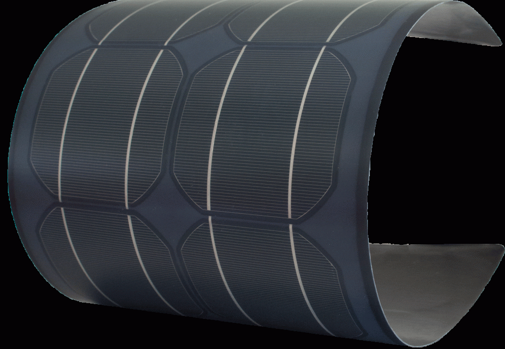
With the full arrival of the mobile energy era, the thin film solar industry grows explosively. Thin-film solar chips are light, thin, and flexible. They can be embedded in various types of carriers like Intel chips, from urban skyscrapers to neighborhood roofs, or parasols on the street, and cars running on the road. They have turned traditional products into “power generation bodies”, enabling energy sharing and free use.

Indium

Indium is one of the basic raw materials for the manufacture of thin film solar cells. Indium, atomic number 49, was discovered in 1863 by the German chemist H. Richter in zinc concentrate. Indium is silvery white and has a light blue color. The texture is very soft and can be scored with nails. In nature, indium minerals are dispersed in trace amounts in other minerals. The distribution of indium in the earth’s crust is relatively small, 1/8 of gold and 1/50 of silver. So far, no single or indium-based natural indium deposit has been found. Therefore, indium resources, in people’s impression, are scarce and difficult to mine, so that there is concern about whether there will be shortages and unstable prices of the precious metal.

Luckily, it is optimistic that the industry has said that with the improvement of mining technology, drilling technology, purification technology and recycling technology, more and more indium resources can be used. Therefore, even if the output of copper indium gallium selenide (CIGS) increases explosively in the next few years, it is difficult to affect the supply and demand of indium.

CIGS solar cell

CIGS solar cellIn the future, the copper indium gallium selenide film industry will enter a period of low-cost and high-speed development, and the thin-film solar market will be fully opened. As the photovoltaic industry continues to evolve, reducing power generation costs is a continuing goal. In this context, reducing the amount of precious indium through technical routes is a cost-reduction method that many companies are actively exploring.

At present, some companies have developed a more reliable solution to reduce the amount of indium used in copper-indium-gallium-selenide modules: developing new plasma-spray target technology, reducing the loss in sputtering target coating, reclaiming indium on residual targets, and etc. In addition, by appropriately increasing the composition of gallium or thinning the battery film layer in the copper indium gallium selenide battery, the amount of indium can also be effectively reduced.

The industry produces metal indium by purifying waste zinc and waste tin, and the recovery rate is about 60-70%. From this calculation, based on the proven reserves, the increase in recoverable amount and the indium recovery rate, the currently available indium is about 15,000 tons to 18,000 tons. If all of these indiums are used to produce copper indium gallium selenide batteries, it can produce 1,800 GW, and even if only one-tenth of the amount is used, it can produce 180 GW. In conclusion, in terms of current copper indium gallium selenide production capacity, indium resources are still very rich.

For more information about thin film coating, please visit https://www.sputtertargets.net/.