6 Facts About Semiconductor Wafers

1. Semiconductor, as it literally seems to be, is a solid substance whose conductivity is between insulators and most metals, either due to the addition of an impurity or because of temperature effects. In other words, the conductivity of the semiconductor can be controlled by adding impurities as a specific amount of other materials to the semiconductor.

2. Most semiconductor wafers are made of silicon, which is the second-most abundant element in the Earth’s crust (about 28% by mass) after oxygen and the eighth-most common element in the entire universe by mass. In addition to silicon, semiconductors also use other materials, including germanium, gallium arsenide, germanium, indium phosphide, sapphire and quartz.

3. Semiconductor wafers are available in a spread of diameters. The first semiconductor wafer made in the US in 1960 was just 1 inch in diameter. Today, standard semiconductor wafers go up from 12 inches to 18 inches.

4. Water is the key component of manufacturing Silicon wafers. It is a compound that basically is a general solvent for all substances, silicon included. A large production facility uses up to 4.8 million gallons of water every day to supply Silicon wafers for manufacturing needs and supply.

5. The thickness of semiconductor wafers varies greatly. The thickness of the wafer is always determined by the mechanical strength of any material used to make it. Regardless of what the semiconductor is made of, the wafer must be thick enough to support its own weight so that it does not break during processing.

6. Contamination is inevitable during the manufacture and transportation of semiconductors. Appropriate storage conditions must be in place to prevent contamination and/or degradation after shipment. Semiconductor wafers that are not vacuum sealed must be placed in a Nitrogen (N2) cabinet at a flow rate of 2 to 6 SCFH (Standard Cubic Feet per Hour).

Stanford Advanced Materials (SAM) is a global sputtering targets manufacturer which supplies high-quality and consistent products to meet our customers’ R&D and production needs. Please visit https://www.sputtertargets.net/ for more information.

Application of Molybdenum Target in Mobile Phone LCD Screen

Nowadays, society is full of phubbers, and mobile phones have become the most indispensable thing for the masses. Mobile phone displays are also becoming more and more high-end, such as full-screen design, small bang design, and so on.

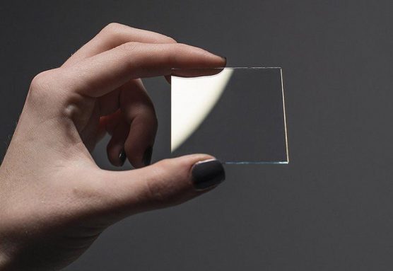
Do you know what the important step is in making a mobile phone LCD screen? — Coating, using magnetron sputtering to sputter metal molybdenum from the molybdenum target onto the liquid crystal glass.

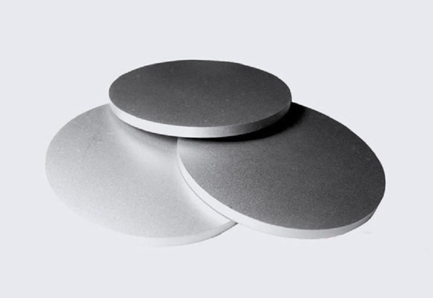
As an advanced film material preparation technology, sputtering has two characteristics of “high speed” and “low temperature”. It concentrates ions into a high-speed ion stream in a vacuum to bombard a solid surface. The kinetic energy exchange between the ions and the atoms on the solid surface causes the atoms on the solid surface to leave the target and deposit on the surface of the substrate to form a nano (or micro) film. The bombarded solid is a material for depositing a thin film by sputtering, which is called a sputtering target.

In the electronics industry, molybdenum sputtering targets are mainly used for flat panel displays, electrodes and wiring materials for thin film solar cells, and barrier materials for semiconductors. These are based on its high melting point, high electrical conductivity, low specific impedance, good corrosion resistance, and good environmental performance.

Molybdenum used in components of LCDs can greatly improve the brightness, contrast, color, and life of the LCD. One of the major applications for molybdenum sputtering targets in the flat panel display industry is in the TFT-LCD field.

molybdenum target

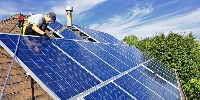
In addition to the flat panel display industry, with the development of the new energy industry, the application of molybdenum sputtering targets on thin film solar photovoltaic cells is also increasing. The molybdenum sputtering target mainly forms a CIGS (Copper Indium Gallium Selenide) thin-film battery electrode layer by sputtering. Among them, molybdenum is at the bottom of the solar cell, and is a back contact of the solar cell. It plays an important role in the nucleation, growth, and morphology of the CIGS thin film crystal.

Stanford Advanced Materials(SAM) is a global sputtering targets manufacturer which supplies high-quality and consistent products to meet our customers’ R&D and production needs. Please visit https://www.sputtertargets.net/ for more information.

3 Minutes to Know PVD Gold Sputtering

Gold is a popular precious metal that has been used for centuries as currency, hedging and jewelry for its noble and beautiful gold color.

PVD Gold Sputtering

Gold sputtering coating is a thin film deposition process in which gold or gold alloy is bombarded with high-energy ions in a vacuum chamber, causing gold atoms or molecules to be “sputtered” into the vapor and condensed on the substrate to be coated. Sputtering is one method of the PVD (Physical Vapor Deposition) process, the other two of which are thermal evaporation deposition and electron beam vapor deposition, and gold is also applied in these two methods. In thermal evaporation deposition, gold evaporates in a low-pressure environment with resistive heating elements; and in electron beam vapor deposition, gold is heated by an electron beam, and then condensed on the substrate to be coated.

Gold Plating

Apart from PVD coating, there are other ways for gold coatings such as gold plating and gold filling. Gold plating is a method that deposits a thin layer of gold on the surface of another metal by chemical or electrochemical plating. The advantages of gold plating are inexpensive and easy. However, the coating it produces is relatively soft and less durable, and what’s worse, its chemical process would cause pollution that is far away from environmentally friendly.

Gold Filling

Gold filling is the mechanical bonding of gold to metal under high temperatures and pressure. It produces a thicker coating than PVD gold sputtering and gold plating, and thus it is usually more expensive.

Advantages of PVD gold sputtering

The constant contact of skin or clothing may abrade the coatings, especially in the watch and jewelry industry. Thus, PVD gold sputtering is preferred in these two industries because the coatings it produces are harder and more durable than that of electrolytic gold plating or gold filling.

Compared to other types of gold coatings, the main advantages of PVD gold sputtering coating are their durability, retention of gloss, corrosion resistance, and abrasion resistance in contact with the skin, thus extending the life of the jewelry. PVD gold sputtering not only provides the exact color and brightness which evokes the general feeling of love and attraction with jewelry, but also has the advantage of being more environmentally friendly and durable than gold plating or gold filling for producing a gold coating.

Stanford Advanced Materials(SAM) is a global sputtering targets manufacturer which supplies high-quality and consistent products to meet our customers’ R&D and production needs.

Pros & Cons of 4 Film Manufacturing Methods

The properties of the thin film are determined by the manufacturing method, and different methods have their own advantages and disadvantages. Commonly used preparation processes include magnetron sputtering, chemical vapor deposition, vacuum evaporation, pulsed laser deposition, etc. Among them, magnetron sputtering deposition technology has been widely researched and applied due to its high film formation rate and good uniformity.

thinfilm_main

Magnetron Sputtering

The basic principle of the method is that under the action of electric and magnetic fields, the accelerated high-energy particles (A, +) bombard the surface of the target, and after the energy is exchanged, the atoms on the surface of the target escape from the original lattice, and finally, the sputtering particles are deposited on the surface of the substrate and react with oxygen atoms to form an oxide film. The magnetron sputtering process is characterized by excellent optical and electrical properties of the film deposited at low temperatures. In addition, it has the advantages of a high deposition rate, low substrate temperature, good film adhesion, easy to control, and large-area film formation. Therefore, it has become the most researched and widely used film-forming technology in industrial production today as well as a research hotspot in ITO film preparation technology.

Chemical Vapor Deposition

The chemical vapor deposition method is a process in which a gaseous reactant (including a gaseous reactant that becomes a vaporized condensed matter after evaporation) is chemically reacted on the surface of the substrate to deposit a film. This chemical reaction occurring on the surface of the substrate is usually the thermal decomposition and in-situ oxidation of the source material. The reaction system selected by the CVD method must satisfy:

(1) At the deposition temperature, the reactant must have a sufficiently high vapor pressure;
(2) The chemical reaction product must be in a gaseous state except for the solid matter deposited on the substrate;
(3) The vapor pressure of the deposit should be low enough to ensure good adsorption on a substrate having a certain temperature.

Vacuum Evaporation

The vacuum evaporation method is a method in which a raw material of a to-be-formed film in an evaporation vessel is vaporized from a surface to form a vapor stream, and is incident on a surface of the substrate to react with a gas to form a film in a vacuum chamber. A high-quality ITO film can be prepared by the electron beam evaporation deposition method, in which the evaporation substance is In2Odoped with SnO2, and the mass percentage of SnO2 is 10%. Under suitable process conditions, the deposited film has a minimum resistivity of 4×10⁻⁴ Ω•cm and an average transmittance in the visible range of more than 90%.

Pulsed Laser Deposition

The pulsed laser deposition (PLD) process is a very competitive new vacuum physical deposition process developed in recent years. Compared with other processes, it has the advantages of precise control of stoichiometry, synthesis, and deposition, and no requirement for the shape and surface quality of the target, so the surface of the solid material can be processed without affecting the material body.

Stanford Advanced Materials(SAM) is a global sputtering targets manufacturer which supplies high-quality and consistent products to meet our customers’ R&D and production needs. Please visit https://www.sputtertargets.net/ for more information.

Selection of Common Coating Types of PVD Coating

Physical Vapor Deposition (PVD) is a thin film preparation technique that physically vaporizes the surface of a material source (solid or liquid) into gaseous atoms, molecules, or partially ionized into ions under vacuum conditions. [1]

Achieving a cost-effective application of the coating depends on a number of factors, and for each particular processing application, there is typically only one or several possible coating options. The choice of coating and its characteristics correctly determines the difference between a significant increase in processability and little improvement. Therefore, it is necessary to select a suitable coating according to detailed parameters such as the processing speed, the cooling method, the material to be processed, and the processing method. The following is our recommended coating selection:

TiN

TiN is a versatile coating that increases tool hardness and has a higher oxidation temperature.

Uses: high-speed steel cutting tools, slow processing tools (such as low-speed turning tools), wear parts, injection molds.

TiCN

The TiCN coating is based on the addition of carbon to the TiN to increase the hardness and low coefficient of friction of the coating.

Uses: high-speed steel tools, stamping dies, forming dies

TiAlN, AlTiN

The alumina coating formed by the TiAlN/AlTiN coating during processing can effectively improve the high-temperature processing life of the processing tool. The high-temperature oxidation resistance of the AlTiN coating is about 100 degrees higher than that of TiAlN.

Uses: Carbide tools (TiAlN is recommended when the hardness of the processed material is lower than HRC45 and AlTiN is recommended when the hardness of the processed material is higher than HRC45), thin-walled stamping die (TiAlN), die-casting die (AlTiN)

CrN

CrN coating has good adhesion, corrosion resistance, and wear-resistance.

Uses: processing aluminum alloy, red copper cutter, injection mold, parts (especially with lubricating oil soaking)

CBC(DLC)

The PLATIT CBC coating is composed of a TIN+TICN+DLC structure. It has the advantages of low friction coefficient, wear-resistance, and low stress of the film layer.

Uses: Lubricating coatings, forming dies, aluminum alloys, and other bonding materials stamping dies.

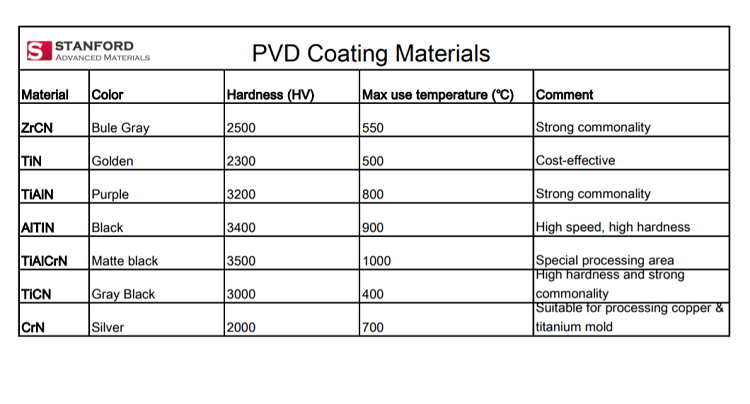
Apart from features and uses, different coating materials also show different colors. If you require the specific color of your coating, you can refer to the sheet below to choose your desirable coating materials.

PVD Coating Colors

Stanford Advanced Materials(SAM) supplies high-quality and consistent products to meet our customers’ R&D and production needs. All the types we talked about above can be found in SAM. Please visit https://www.sputtertargets.net/ for more information.

Reference:

[1] What is Physical Vapor Deposition (PVD)?

PVD Coating: Give Your Watch a Durable Coat

For most people who could not afford a pure gold watch, a gold coating may be a good choice for them. However, since it is a thin film coating, it is inevitable that the gold color would fade out. So the primary consideration in choosing the coating material/method is durability. If you want to give your watch a durable coat, you really should think about PVD coating.

What is PVD coating?

PVD coating, or Physical Vapor Deposition, refers to a variety of vacuum deposition techniques where solid metal is vaporized to produce thin films and coating. The main methods of physical vapor deposition include vacuum evaporationsputtering depositionarc plasma platingion plating, etc. PVD film has fast deposition speed as well as strong adhesion, good diffraction, and a wide application range.

Maybe you will find it not easy to understand it since PVD is a physical terminology. But actually, as a watch lover, you should just know that PVD coating can provide a metal coat to your watch, making it more beautiful and durable.

Why should you choose PVD coating?

PVD coating has high hardness, high wear resistance, low friction coefficient, good corrosion resistance, and chemical stability. So PVD coating would definitely have a longer lifetime than other traditional coatings. Apart from durability, PVD coating provides multiple kinds of metallic colors, such as gold(TiN), rose gold(TiAlN), silver(Cr2N), brass(ZrN), light grey(TiC), and so on. You will always find the one you like.

PVD Coating Colors

More tips

If you are going to give your watch a PVD coating after reading this blog, I’d like to help you save time in choosing the coating materials. Please consider Stanford Advanced Materials (SAM), which is a global supplier of various technical-grade coating materials as well as high-purity chemicals (up to 99.99999%). All of the coating materials we talked about above can be found on SAM’s website. We ensure that you can get your watch the most durable coat here.

What is Reactive Sputtering Coating Technology?

At present, reactive sputtering deposition is a well-established sputter coating technology and is widely used for industrial coating deposition to produce thin layers for high-added value products, such as flat panel displays, solar cells, optical components, and decorative finishes.

Definition

In the process of reactive sputtering, a target material is sputtered in the presence of a gas or a mixture of gasses that will react with the target material to prepare a compound film of a predetermined chemical ratio. Reactive sputtering is most often practiced using one or more magnetron sputtering cathodes. Therefore, it is also called reactive magnetron sputtering.

Sputtering Target

Sputtering targets can be divided into metal targets, alloy targets, ceramic targets, etc. Metal sputtering targets can be used to produce compound materials. For example, a titanium sputtering target can be used to produce coatings such as TiO2, TiN, and Ti-O-N. Apart from it, titanium targets can also be used to produce any of the aforementioned different compositions as well as boride and carbide films. Compared with the compound target, the metal target has the advantage of longer service life.

Reactive gases

In most cases, Argon is the main gas used in reactive sputtering as well as other sputter coating methods. It has to be mentioned that the amount of a reactive gas introduced into a process chamber should be strictly controlled in order to either achieve a certain amount of doping or to produce a fully reacted compound. Here is a list of other gasses used in reactive sputtering).

Gasses Uses
Oxygen (O2) deposition of oxide films (e.g. Al2O3, SiO2, TiO2, HfO2, ZrO2, Nb2O5, AZO, ITO)
Nitrogen (N2) deposition of nitride films (e.g. TiN, ZrN, CrN, AlN, Si3N4, AlCrN, TiAlN)
Carbon dioxide (CO2) deposition of oxide coatings
Acetylene (C2H2) deposition of metal-DLC, hydrogenated carbide, carbo-nitride films
Methane (CH4) similar applications as for C2H2

Several reactive gasses can be mixed in order to deposit a multi-component functional thin film. Additional reactive gas is sometimes used to enhance a certain deposition process (e.g. addition of N2 in the SiO2 reactive sputtering process).

Application

Coatings and films produced by Reactive Magnetron Sputtering can be used in a large variety of products such as OLED devices, optical antireflective coatings, and decorative coatings.

 Please visit https://www.sputtertargets.net/ for information.

Determining Factors For Fillm Uniformity

Sputtering targets are materials that are indispensable during the sputtering process in the coating industry. Uniformity is an indicator used to value the quality of the coated film. Usually, there are two factors that determine the coating uniformity: the length of the targets and the distance between the target and the substrate.

factors that determine the coating uniformity

Length of the sputtering targets

The length of the target is an important factor in producing a coating with good uniformity, because it decides which construction method to be used. It’s better you consider the length of certain monolithic targets during the process requirements planning phase in order to achieve good uniformity.

Suitable target length depends on the orientation of the sputtering target materials and how much weight the target flanges can support without plastically deforming or breaking which can occur for brittle materials. For example, ceramic targets are usually brittle and usually need to be bonded with a backing tube, so the length of ceramic targets cannot be too long, otherwise, they will easily break into pieces. In addition, people usually joined small ceramic targets together to produce the large-area ceramic thin film in the case.

Distance between the target and Substrate

The other factor to define the achievable uniformity of the obtained film is the distance between the sputtering target and the substrate. The larger the distance is, the poorer the uniformity is achieved on the substrate. To be noted, the distance is not stable during the process: it keeps increasing as the target materials keep being consumed and eroding. Therefore, generally speaking, the density of the coating is not uniform, and the worst process uniformity occurs when the sputtering ends.

In general, the distance between the target and the substrate is measured before the start of sputtering, so that the uniformity we calculated is theoretically the best, or the most achievable. But in fact, at the end of the sputtering, the initial uniformity specification could not be reached due to the increase in the distance. The specific difference depends on the initial target thickness.

What Will Affect The Magnetron Sputtering Voltage?

Magnetic field

Magnetic field influences inversely the sputtering voltage. In other words, when the magnetic field on the surface of the sputtering target increases, the operating voltage of magnetron sputtering will decrease. It happens because the sputter-etched surface of the target gets closer to the strong magnetic field of the permanent magnet behind the target. To be noted, when the magnetic field strength increases above 0.1T, its effect on the sputtering voltage is no longer obvious.

In order to reduce the influence of this factor, the thickness of the sputtered material is not arbitrary, but limited. In general, thicker non-magnetic targets can be used in stronger magnetic fields.

magnetron sputtering11-9-2

Material Type

Different target materials also affect the sputtering voltage. Here are examples of ITO, copper, aluminum, titanium, manganese, and chromium target.

Sputtering Target Sputtering Voltage
Indium Tin Oxide (ITO) ≈200V
Copper (Cu)
Aluminum (Al)
Titanium (Ti)
400~600V
Manganese (Mn)
Chromium (Cr)
>700V

Gas Pressure

Working gas pressure

Under the condition that various parameters (such as environmental conditions, power control panel parameters, etc.) remain unchanged, the increase of the working gas pressure will reduce the magnetic sputtering voltage.

Reactive gas pressure

On contrary, under the determined environment and constant power source, the increase of reactive gas pressure will result in the increase of magnetic sputtering voltage.

Distance Between Cathode & Anode

magnetron sputtering11-9

The distance between the cathode and anode in vacuum gas discharge can have a certain effect on the sputtering voltage. If the distance is too large, the internal resistance of the equivalent gas discharge is mainly determined by the plasma equivalent internal resistance. Conversely, if the distance is too small, the internal resistance of the plasma discharge will be small.

When the magnetron target ignited and enters the normal sputtering, if the distance between the cathode and anode is too small, although the sputtering current has reached the process setting value, the target sputtering voltage is still low.

Please visit https://www.sputtertargets.net/ for more information.

Application and Recycling of Tungsten Metals

Tungsten, a relatively rare and exotic metal, has been widely used in many products in our daily life. Tungsten has the advantages of high melting point, high hardness, excellent corrosion resistance, and good electrical and thermal conductivity. Most of its applications are based on these properties. Tungsten is not cheap because of its scarcity, but the price of tungsten is quite reasonable compared with the prices of other rare and exotic metals.

What are the Applications of Tungsten?

Tungsten is an important alloying element for the aerospace industry and the industrial gas turbine industry, because it can significantly improve the strength, hardness, and wear resistance of steel.

Tungsten filament is used in incandescent bulbs to replace tantalum, which was used many years ago, as an integral part of copper and silver electrical contacts for improved wear resistance.  Tungsten wire can also be used to manufacture direct heating cathodes and grids of electronic oscillation tubes and cathode heaters in various electronic instruments.

Tungsten sputtering target & Ta evaporation pellets can be used as wear-resistant coatings for mechanical parts, as evaporating filaments for physical vapor deposition (PVD) of aluminum and silver, and as key barrier electrons for barrier coatings in critical electronic devices.

Some of the other applications of Tungsten include the component of chemicals and catalysts, cutting blades, paints, pigments, inks, lubricants, etc.

How to Recycle Tungsten?

Tungsten’s unique properties of heavy weight, high hardness, and high melting point make tungsten waste ideal for recycling. The fact that it is chemically resistant is a key factor in tungsten recycling. Therefore, recycling tungsten-bearing scrap is more popular. The methods of tungsten recycling can be roughly divided into the direct method and the indirect method.

Direct Tungsten Recycling

The direct method means that the tungsten waste is converted into a powder of the same composition by chemical or physical treatment or a combination of both. A typical example of a direct method is a zinc treatment method. This method has many advantages, such as limited energy consumption and chemical waste, as well as low production costs. A disadvantage of this method is the limitation on recycled materials.

Indirect Tungsten Recycling

Indirect methods, such as wet chemical processing, are commonly used in refining processes. This type of recycling has no restrictions on materials, but requires a lot of chemicals and energy.

For more information, please visit https://www.sputtertargets.net/.