Advantages of Germanium Sputtering Targets in Infrared Optics

Germanium Sputtering Targets play a pivotal role in the world of infrared optics, significantly enhancing the performance of devices used in various applications, from night vision systems to thermal imaging cameras. In this article, we’ll explore the unique advantages that Germanium Sputtering Targets offer in the realm of infrared optics.

Enhanced Infrared Absorption:

One of the standout features of Germanium Sputtering Targets is their exceptional ability to absorb infrared radiation. This property makes them indispensable for the creation of lenses, windows, and optical components used in infrared imaging systems. Germanium’s high refractive index in the infrared spectrum allows for minimal light reflection, ensuring that more incident light is captured and utilized, resulting in clearer and sharper images.

Broad Infrared Transparency:

While Germanium is an excellent absorber of infrared radiation, it is also transparent to a wide range of infrared wavelengths. This unique combination of absorption and transparency makes Germanium Sputtering Targets ideal for antireflection coatings on optical surfaces. By applying a thin layer of Germanium, manufacturers can reduce unwanted reflections and increase the overall transmittance of their infrared optics.

Resistance to Thermal Stress:

Infrared optical devices often operate in demanding environments where temperature fluctuations are common. Germanium Sputtering Targets are renowned for their resistance to thermal stress, allowing them to maintain their optical performance even under extreme temperature conditions. This property is crucial for ensuring the reliability and longevity of infrared optics used in aerospace, defense, and industrial applications.

Precise Thin Film Deposition:

Germanium Sputtering Targets are used in the physical vapor deposition (PVD) process to create high-quality thin films on various substrates. This precision allows manufacturers to engineer optical coatings with specific infrared properties, such as anti-reflective coatings or filters that target specific wavelengths. Such tailored coatings are essential for optimizing the performance of infrared optical systems.

Applications in Night Vision Technology:

Night vision devices rely heavily on Germanium lenses and windows. The ability to capture and transmit infrared light enables these devices to provide clear images in low-light or no-light conditions. Whether used by military personnel, law enforcement agencies, or wildlife enthusiasts, Germanium-based optics are at the heart of night vision technology.

For more information about germanium sputtering targets and other target materials, please visit https://sputtertargets.net/.

Spherical Nickel Powder vs. Traditional Nickel Powder: A Comparative Analysis

In the realm of metal powders, nickel holds a significant place due to its versatility and wide-ranging applications. Recently, the emergence of spherical nickel powder has sparked considerable interest, prompting comparisons with traditional nickel powder. In this article, we delve into the distinctions between these two forms of nickel powder and explore the scenarios where each shines.

Particle Morphology: Spherical vs. Irregular

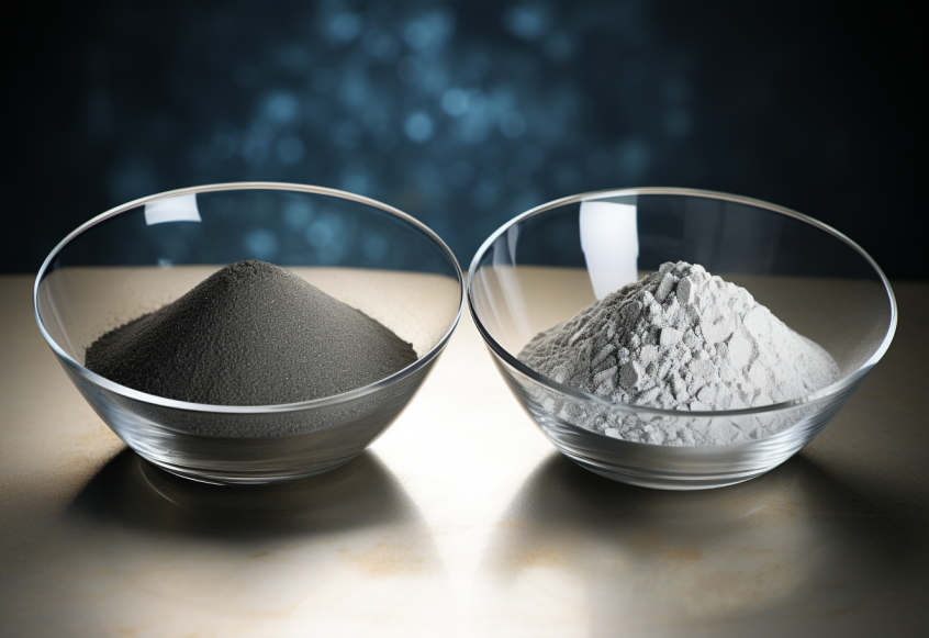
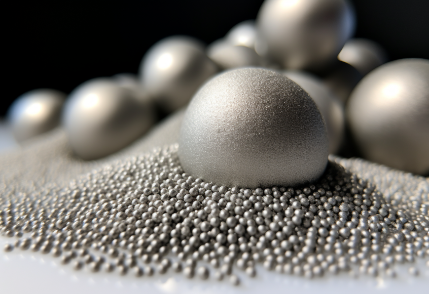
The most noticeable difference between spherical nickel powder and traditional nickel powder lies in their particle morphology. Spherical nickel powder is characterized by its uniform, spherical particle shape, while traditional nickel powder consists of irregularly shaped particles. This distinction plays a pivotal role in various aspects of their performance and applications.

Flowability and Packing Density

Spherical nickel powder’s uniform shape offers enhanced flowability and packing density. During manufacturing processes like additive manufacturing, the particles flow smoothly and evenly, resulting in higher material utilization and reduced powder wastage. In contrast, traditional nickel powder’s irregular particles can lead to uneven flow, resulting in challenges during processing and decreased packing density.

Porosity and Structural Integrity

The shape of nickel powder particles directly impacts the porosity and structural integrity of the final product. Spherical nickel powder’s uniform packing leads to reduced porosity and improved mechanical properties. This makes it an excellent choice for applications where high strength and dimensional accuracy are paramount. Traditional nickel powder, due to its irregular particles, can result in higher porosity levels and reduced structural integrity.

Surface Quality and Finish

Spherical nickel powder’s uniform particle size distribution contributes to smoother surfaces and finer finishes in products. This is particularly crucial in industries where aesthetics and surface quality play a significant role. On the other hand, traditional nickel powder’s irregular particles can lead to rougher surfaces and increased post-processing requirements.

Applications and Industries

The choice between spherical nickel powder and traditional nickel powder largely depends on the specific application and industry requirements. Spherical nickel powder’s advantages make it a prime candidate for additive manufacturing, aerospace components, and electronics, where precision and performance are essential. Traditional nickel powder remains relevant in applications that don’t require the same level of uniformity and performance, such as certain types of coatings and metallurgical processes.

The Road Ahead

Both spherical nickel powder and traditional nickel powder have their distinct roles in the realm of material science and manufacturing. As industries continue to innovate and push boundaries, the choice between these two forms of nickel powder will depend on the specific performance criteria, design requirements, and production methods.

In conclusion, the comparison between spherical nickel powder and traditional nickel powder underscores the critical role that particle morphology plays in material performance and applications. While each form has its advantages, the choice ultimately depends on the unique demands of the project and the desired outcome.

For more information about spherical nickel powder or spherical powder for 3d printing, please visit https://www.sputtertargets.net/.

Advantages of Using Spherical Nickel Powder in Additive Manufacturing

Additive manufacturing, commonly known as 3D printing, has ushered in a new era of manufacturing possibilities. Among the various materials used in this innovative technology, spherical nickel powder stands out for its remarkable properties and advantages. In this article, we delve into the world of additive manufacturing and explore the reasons why spherical nickel powder is becoming a game-changer in this field.

The Unique Attributes of Spherical Nickel Powder

Spherical nickel powder possesses a distinct advantage over traditional nickel powder due to its shape and size uniformity. The spherical shape of the particles ensures consistent flowability and improved packing density during the printing process. This leads to enhanced layer-to-layer adhesion and reduced porosity in the printed objects, resulting in parts with higher mechanical strength and improved structural integrity.

Tailoring Material Properties

Additive manufacturing allows engineers and designers to create intricate and complex geometries that were once thought impossible. Spherical nickel powder contributes to this capability by enabling the production of fine, intricate structures with high surface quality. Its uniform particle size distribution ensures an even deposition of layers, leading to smooth surfaces and accurate dimensional accuracy. Moreover, the material’s excellent thermal and electrical conductivity make it ideal for applications requiring heat dissipation and electrical connectivity.

Advancements in Functional Parts

The aerospace and automotive industries are leveraging spherical nickel powder’s unique properties to produce functional parts with exceptional performance characteristics. In aerospace, components like engine turbines and fuel nozzles benefit from the material’s ability to withstand high temperatures and corrosive environments. Similarly, in the automotive sector, the use of spherical nickel powder is contributing to the development of lightweight, high-strength parts that enhance fuel efficiency and overall vehicle performance.

The Path to Sustainability

As industries increasingly focus on sustainability, the role of materials like spherical nickel powder becomes crucial. Its efficient use in additive manufacturing results in minimal material wastage, making it an environmentally friendly choice. Additionally, the potential for recycling and reusing powder not used during printing further reduces material consumption and waste generation.

Challenges and Future Directions

While spherical nickel powder holds immense promise, challenges such as powder handling and production costs remain. Researchers and manufacturers are actively working to overcome these hurdles, paving the way for broader adoption of this advanced material. As additive manufacturing continues to evolve, the synergy between technology and material innovation will likely lead to breakthroughs in both performance and affordability.

In conclusion, spherical nickel powder is transforming the additive manufacturing landscape by offering unparalleled advantages in terms of material properties, design flexibility, and sustainability. Its role in producing functional parts for industries ranging from aerospace to automotive underscores its importance in shaping the future of manufacturing.

For more information about spherical nickel powder or spherical powder for 3d printing, please visit https://www.sputtertargets.net/.

Zinc Oxide Thin Films in Nanotechnology: Synthesis and Applications

Introduction

Zinc oxide (ZnO) is a wide-bandgap semiconductor with diverse properties that have garnered significant attention in nanotechnology research. The synthesis of zinc oxide thin films using sputtering targets has opened up new possibilities for various nanoscale applications. This article explores the synthesis process of ZnO thin films through sputtering and delves into their emerging applications in the field of nanotechnology.

Synthesis of Zinc Oxide Thin Films using Sputtering Targets

Sputtering is a popular thin film deposition technique that involves bombarding a target material with high-energy ions to release atoms or molecules, which then condense on a substrate to form a thin film. The sputtering process for zinc oxide thin films is typically carried out in a vacuum chamber, where an argon plasma is used to dislodge zinc oxide atoms from a sputtering target. The sputtered atoms travel through the vacuum and deposit onto a substrate, forming a thin film.

One of the main advantages of sputtering is the ability to precisely control the thickness and composition of the thin film. This level of control allows researchers to tailor the properties of zinc oxide thin films for specific nanotechnology applications.

Properties of Zinc Oxide Thin Films

Zinc oxide thin films possess several unique properties that make them highly attractive for nanoscale applications. Firstly, ZnO is a wide-bandgap semiconductor, making it suitable for optoelectronic devices such as light-emitting diodes (LEDs) and photodetectors. The wide bandgap allows ZnO thin films to emit and detect light in the ultraviolet region, which is essential for various optical and sensing applications.

Additionally, zinc oxide exhibits excellent piezoelectric properties, meaning it can convert mechanical energy into electrical signals and vice versa. This property has opened up opportunities for ZnO thin films in nanoelectromechanical systems (NEMS) and sensors.

Applications of Zinc Oxide Thin Films in Nanotechnology:

  1. Nanosensors: Zinc oxide thin films are used as sensitive layers in gas sensors and biosensors due to their high surface area and excellent sensing properties. They have been employed in detecting gases such as ammonia, carbon monoxide, and hydrogen, making them valuable for environmental monitoring and medical diagnostics.
  2. Nanodevices: ZnO thin films find applications in the development of nanodevices like field-effect transistors (FETs) and nanogenerators. Their exceptional piezoelectric characteristics make them ideal for energy harvesting applications.
  3. Nanophotonics: Zinc oxide thin films are used in the fabrication of nanophotonic devices, including waveguides and microcavities. Their ability to emit and manipulate light at the nanoscale level makes them essential in advanced optical communication systems.
  4. Nanocoatings: ZnO thin films serve as protective nanocoatings for various surfaces, providing enhanced resistance to environmental factors like UV radiation and corrosion.

Conclusion

Zinc oxide thin films synthesized using ZnO sputtering targets have emerged as a key player in the field of nanotechnology. Their versatile properties and precise synthesis make them ideal for a wide range of nanoscale applications. As researchers continue to explore the unique properties of ZnO thin films, we can expect to see further advancements in nanotechnology, leading to innovative devices and technologies that address various global challenges.

For more information about ZnO sputtering target or other thin film coating materials, please visit https://www.sputtertargets.net/.

Molybdenum Targets in Semiconductor Manufacturing

Introduction

Semiconductor manufacturing is at the heart of modern technology, driving advancements in electronics, telecommunications, and computing. Key to this process is the use of specialized materials and techniques, with molybdenum targets playing a crucial role in thin film deposition. This article delves into the significance of molybdenum targets in semiconductor manufacturing, exploring their applications and advantages in enabling the creation of high-performance electronic devices.

Molybdenum Targets and Thin Film Deposition

Thin film deposition is a fundamental process in semiconductor manufacturing, where thin layers of material are precisely deposited onto a substrate to form integrated circuits and other electronic components. Molybdenum targets, typically in the form of sputtering targets, are vital to this process due to their exceptional material properties. Molybdenum is a refractory metal, offering high melting points and excellent thermal stability, making it suitable for use in demanding high-temperature environments during thin film deposition.

Sputtering is the primary technique employed for depositing thin films using molybdenum targets. In this process, molybdenum atoms are sputtered from the target’s surface through ion bombardment and subsequently deposited onto the substrate. The precise control of this deposition allows for the creation of uniform and well-adhered thin films with precise thicknesses, critical for the functionality of semiconductor devices.

Applications in Semiconductor Devices

Molybdenum targets find widespread use in semiconductor manufacturing for various applications. One of the primary applications is in the creation of gate electrodes in metal-oxide-semiconductor field-effect transistors (MOSFETs). MOSFETs are essential components of integrated circuits, controlling the flow of electrical current and enabling the amplification of signals in electronic devices. The high thermal and electrical conductivity of molybdenum makes it an ideal choice for gate electrodes, ensuring efficient device performance.

Additionally, molybdenum targets are used in the fabrication of interconnects, which serve as conductive pathways between different components on the semiconductor device. The high purity and uniformity of molybdenum thin films are critical for achieving low electrical resistance in interconnects, minimizing power losses and improving the overall efficiency of electronic devices.

Advantages of Molybdenum Targets

Several key advantages make molybdenum targets stand out in semiconductor manufacturing:

  1. Thermal Stability: Molybdenum targets can withstand high temperatures, ensuring stability during the deposition process. This is particularly important for high-temperature processing steps in semiconductor manufacturing.
  2. High Purity: The exceptional purity levels of molybdenum targets enable the deposition of clean and contamination-free thin films, resulting in reliable semiconductor devices with consistent performance.
  3. Uniformity: Molybdenum targets facilitate the creation of uniform thin films, ensuring consistent device characteristics across a wafer and improving the overall yield of the manufacturing process.
  4. Compatibility: Molybdenum targets are compatible with various deposition techniques, offering flexibility in thin film deposition processes for different semiconductor applications.

Conclusion

In conclusion, molybdenum targets play a critical role in semiconductor manufacturing by enabling precise thin film deposition. Their exceptional thermal stability, high purity, and uniformity make them indispensable for the creation of high-performance semiconductor devices. From MOSFET gate electrodes to interconnects, molybdenum targets contribute to the advancement of modern technology, ensuring reliable and efficient electronic devices that power our digital world. As semiconductor technology continues to evolve, molybdenum targets will remain at the forefront, driving innovation and shaping the future of electronics.

For more information about molybdnem sputtering target or other target materials, please visit https://www.sputtertargets.net/.

Essential Terms for Sputtering and Evaporation Processe

Terminologies of Sputtering Coating

General Term

  1. Vacuum deposition: A group of methods used to deposit layers of material under a vacuum.
  2. Substrate: The material on which the film is deposited.
  3. Coating material: The raw material used to deposit the film, including sputtering targets and evaporation pellets materials.
  4. Sputtering target: A coating material used for sputtering in vacuum sputtering.
  5. Sputtering rate: The amount of sputtering material used over a given time interval divided by the time interval.
  6. Deposition rate: The amount of material deposited on the substrate over a given time interval divided by the time interval and the surface area of ​​the substrate.

Information from SAM Sputter Target, a global coating materials supplier.

Technical Terminology

  1. Vacuum sputtering: The process by which inert gas ions bombard atoms (molecules) or radicals from the target surface in a vacuum.
  2. Reactive vacuum sputtering: Vacuum sputtering of film material of a desired chemical composition by reaction with a gas.
  3. Direct current diode sputtering: A direct current voltage between two electrodes causes the gas to self-sustain and discharge the target as a cathode.
  4. High-frequency diode sputtering: A high-frequency discharge is obtained by a high-frequency voltage between two electrodes to cause sputtering of a negative potential at a target.
  5. Ion beam sputtering: An ion beam obtained by a special ion source causes the sputtering of a target.
  6. Magnetron sputtering: The secondary electrons are bound to specific areas of the target surface using an orthogonal electromagnetic field formed on the surface of the target to enhance ionization efficiency and increase ion density and energy. Therefore, a very high sputtering rate can be obtained at a low voltage and a large current.

Special Parts

  1. Sputtering device: The components of a vacuum sputtering apparatus including a target and an auxiliary device necessary for sputtering (for example, a power supply device, a gas introduction device, etc.).
  2. Sputtering Target: The surface is bombarded with particles. The meaning of the target in this standard is the electrode composed of the sputtering material in the sputtering apparatus.
  3. Shutter: A device used to limit the coating in time and/or space and thereby achieve a certain film thickness distribution. The baffle can be either fixed or movable.
  4. Mask: A device used to cover part of the substrate and to limit the coating in space.
  5. Substrate heating device: A device that can heat a substrate or substrates to the desired temperature by heating in a vacuum coating device.
  6. Substrate cooling device: In a vacuum coating device, a device achieves the desired temperature by cooling a substrate or substrates.

Terminologies of Vacuum Evaporation

General Term

  1. Vacuum coating: A method of making a film on a substrate under vacuum.
  2. Substrate: The surface on which the film is deposited.
  3. Testing substrate: A substrate used for measurement and/or testing at the beginning of coating, during the coating process, and after coating.
  4. Coating material: The raw material used to make the film, mainly including sputtering targets and evaporation pellets materials.
  5. Evaporation material: A coating material used for evaporation in vacuum evaporation.
  6. Film material: the material constituting the film layer.
  7. Evaporation rate: the amount of material evaporated during a given time interval divided by
  8. Deposition rate: The amount of material deposited on a substrate over a given time interval divided by the time interval and the surface area of ​​the substrate.
  9. Coating angle: The angle between the direction of the particles incident on the substrate and the normal to the surface being plated.

Information from SAM Sputter Target, a global coating materials supplier.

Technical Terminology

  1. Vacuum evaporation coating: A vacuum coating process for evaporating a coating material.
  2. Simultaneous evaporation: Vacuum evaporation of various evaporation materials simultaneously onto the substrate by several evaporators.
  3. Evaporation field evaporation: Evaporation of a material evaporated from the evaporation field onto a substrate for evaporation (this process is applied to large-area evaporation to obtain a desired film thickness distribution).
  4. Reactive vacuum evaporation: Vacuum evaporation of film material of a desired chemical composition by reaction with a gas.
  5. Reactive vacuum evaporation in evaporator: Reacts with various evaporation materials in the evaporator to obtain vacuum evaporation of the desired chemical composition film material.
  6. Direct heating evaporation: The heat necessary to evaporate the evaporation of the material is the same as the heat of the evaporation material (in the crucible or not).
  7. Induction heating evaporation: The evaporation material is heated by induction eddy current.
  8. Electron beam evaporation: evaporation of heated material by electron bombardment.
  9. Laser beam evaporation: evaporation of the material by laser beam heating.
  10. Indirect heating evaporation: In a heating device (for example, a boat-shaped evaporator, a crucible, a filament, a heating plate, a heating rod, a spiral coil, etc.), the evaporation material is subjected to the heat necessary for evaporation, and is transferred to the evaporation material by heat conduction or heat radiation.
  11. Flash evaporation: intermittently evaporate a very small amount of evaporating material.

Special Parts

  1. Coating chamber: A part of a vacuum coating equipment that performs the actual coating process.
  2. Evaporator device: A vacuum coating device that includes an evaporator and all components necessary for its operation (such as power supply, supply, cooling devices, etc.).
  3. Evaporator: A device that evaporates directly within it, such as a boat-shaped evaporator, crucible, filament, heating plate, heating rod, spiral coil, etc., and if necessary, the evaporation material itself.
  4. Evaporator by direct heat: An evaporator in which the evaporation material itself is heated.
  5. Evaporator by indirect heat: An evaporator in which an evaporation material is heated by heat conduction or heat radiation.
  6. Evaporation field: A field formed by heating the same vaporized material by several arrays of evaporators.

Enhancing PV Device Efficiency with Indium Sputtering Targets

Introduction

Indium sputtering targets play a crucial role in the fabrication of photovoltaic (PV) devices, enhancing solar energy conversion efficiency. In this article, we discuss the advantages and applications of indium sputtering targets in improving the performance of PV devices.

Transparent Conductive Oxide (TCO) Layers

Indium sputtering targets are used to deposit high-quality indium tin oxide (ITO) films onto solar cells. These transparent conductive oxide layers offer excellent electrical conductivity and allow for light transmission, enhancing solar energy conversion efficiency.

Anti-Reflective Coatings

Indium sputtering targets enable the deposition of indium oxide or indium-tin-oxide thin films as anti-reflective coatings. These coatings minimize reflection losses, optimizing light absorption in PV devices and increasing overall energy conversion efficiency.

Back Contact Layers

Indium sputtering targets are utilized in depositing back contact layers in PV devices. These layers, made of indium or indium-containing compounds, improve charge collection and extraction, leading to enhanced power output and device performance.

Doping Layers

With indium sputtering targets, indium-containing films can be deposited as doping layers in PV devices. Doping with indium allows for better control of carrier concentration, facilitating efficient charge separation and collection, and improving solar energy conversion efficiency.

Conclusion

The use of indium sputtering targets in PV device fabrication enhances solar energy conversion efficiency. By enabling the deposition of transparent conductive oxide layers, anti-reflective coatings, back contact layers, and doping layers, indium sputtering targets optimize various aspects of PV device performance. As solar energy gains prominence as a clean and renewable energy source, the demand for indium sputtering targets in PV applications will continue to grow, driving further advancements in solar energy conversion technology.

For more information about indium sputter targets or other types of sputtering materials, please visit https://www.sputtertargets.net/.

Properties, Fabrication, and Applications of Indium Sputtering Targets in Thin Film Deposition

Introduction

Indium is a soft silvery-white metal that possesses unique properties, making it a valuable material in various fields of science and industry. One of the primary applications of indium is in thin film deposition. In this article, we will explore the properties of indium sputtering targets, their fabrication methods, and their wide-ranging applications in thin film deposition processes.

Properties of Indium Sputtering Targets

Indium sputtering targets exhibit several key properties that make them suitable for thin film deposition:

  1. Purity: High-purity indium sputtering targets are essential to ensure the quality and reliability of the deposited films. Typically, indium targets with purity levels greater than 99.99% are used to minimize impurities and enhance film performance.
  2. Density and Homogeneity: The density and homogeneity of the sputtering target play a vital role in achieving uniform film deposition. Indium targets with high density and excellent homogeneity ensure consistent film thickness and composition across the substrate.
  3. Grain Structure: The grain structure of indium sputtering targets affects their thermal and electrical conductivity. Fine-grained indium targets promote better electrical contact and heat transfer during the sputtering process, leading to improved film properties.

Fabrication of Indium Sputtering Targets

The fabrication process of indium sputtering targets involves the following steps:

  1. Melting and Casting: High-purity indium is melted in a controlled environment to remove any impurities. The molten metal is then cast into solid ingots or other desired shapes, such as discs or rectangles, depending on the specific requirements of the thin film deposition system.
  2. Hot/Cold Rolling: The cast indium ingots undergo hot or cold rolling processes to achieve the desired thickness and dimensions for sputtering target manufacturing. This step helps in improving the density and homogeneity of the indium targets.
  3. Annealing: Annealing is performed to relieve any residual stress and enhance the mechanical properties and grain structure of the indium sputtering targets. Controlled heating and cooling processes are employed to ensure optimal annealing conditions.
  4. Machining: The rolled and annealed indium sheets are machined to obtain the final shape and size of the sputtering target. Precision machining techniques such as cutting, grinding, and polishing are employed to achieve the required surface finish and dimensional accuracy.

Applications of Indium Sputtering Targets in Thin Film Deposition

Indium sputtering targets find wide-ranging applications in various thin film deposition techniques, including:

  1. Optoelectronic Devices: Indium tin oxide (ITO) films deposited using indium sputtering targets are extensively used in touchscreens, flat panel displays, and solar cells due to their excellent electrical conductivity and optical transparency.
  2. Semiconductor Industry: Indium sputtering targets are employed in the deposition of indium-based compounds, such as indium gallium arsenide (InGaAs), indium phosphide (InP), and indium antimonide (InSb), which are crucial for advanced semiconductor devices like high-speed transistors and infrared detectors.
  3. Superconducting Films: Indium sputtering targets are utilized in the deposition of superconducting films, specifically indium-based superconductors, which exhibit zero electrical resistance at low temperatures. Such films are significant in the development of high-performance electronic devices and quantum computing applications.
  4. Transparent Conductive Films: Indium sputtering targets are also employed to deposit transparent conductive films on glass or plastic substrates. These films find applications in organic light-emitting diodes (OLEDs), smart windows, and electromagnetic shielding films.

Conclusion

Indium sputtering targets offer valuable properties for thin film deposition, including high purity, density, homogeneity, and fine grain structure. The fabrication process ensures the production of high-quality targets suitable for diverse applications in optoelectronics, semiconductors, superconductors, and transparent conductive films. As technology advances, the demand for indium sputtering targets is likely to grow, contributing to further innovations in thin film deposition and related industries.

For more information about indium sputter targets or other types of sputtering materials, please visit https://www.sputtertargets.net/.

Exploring the Specific Uses of Zirconium Targets and Thin Films in Different Industries

Zirconium targets and thin films are versatile materials that find a wide range of applications in different industries. With their high melting point, good thermal conductivity, and resistance to corrosion and wear, zirconium-based coatings offer unique properties that make them ideal for use in many different applications.

Semiconductor Industry

Zirconium targets find extensive use in the semiconductor industry for creating thin films with excellent uniformity and purity. In semiconductor manufacturing, zirconium-based coatings are used as diffusion barriers in copper interconnects and as adhesion layers between metal contacts and dielectric layers. These coatings help to enhance the performance, reliability, and durability of semiconductor devices by preventing unwanted chemical reactions, improving electrical conductivity, and enabling precise control of the thickness and composition of each layer.

Energy Industry

Zirconium targets and thin films find significant applications in the energy industry, particularly in solar panel manufacturing. Zirconium-based coatings are applied to solar panels to improve their efficiency by reducing the reflection of sunlight and enhancing light absorption. Zirconium-based coatings also provide corrosion resistance, enabling the solar panels to withstand harsh environments and extend their lifespan. In nuclear power plants, zirconium alloys are used as fuel cladding in the core of reactors due to their excellent corrosion resistance and mechanical strength.

Automotive Industry

Zirconium targets and thin films are used in the automotive industry for coating engine components to improve their wear resistance, hardness, and corrosion protection. Zirconium-based coatings can be applied to automotive parts such as valves, pistons, and bearings to reduce friction and wear, leading to improved fuel efficiency and reduced emissions. Zirconium-based coatings can also provide excellent corrosion protection, enabling automotive parts to withstand harsh environments and extend their service life.

Medical Industry

Zirconium targets and thin films find extensive applications in the medical industry due to their biocompatibility, durability, and corrosion resistance. Zirconium-based coatings are used in orthopedic and dental implants to enhance implant stability, reduce wear and inflammation, and promote bone integration. Zirconium-based coatings can also be applied to medical devices such as surgical instruments and pacemakers to improve their wear resistance and corrosion protection, leading to extended service life and improved patient outcomes.

Aerospace Industry

Zirconium targets and thin films are used in the aerospace industry for coating various components to improve durability and corrosion protection. Zirconium-based coatings are applied to turbine blades, engine parts, and airframe structures to reduce wear, improve fatigue resistance, and enhance corrosion protection. Zirconium-based coatings can also be used as a thermal barrier for components exposed to high temperatures, improving their performance and extending their lifespan.

Conclusion

In summary, zirconium targets and thin films find diverse applications in different industries due to their unique properties and versatility. From semiconductor manufacturing to aerospace engineering, zirconium-based coatings offer numerous benefits such as improved uniformity, purity, durability, wear resistance, and corrosion protection. As research and development continue to advance, zirconium targets and thin films are likely to become an even more important material in many industries.

Read more at sputtertargets.net.

Unlocking the Benefits of Zirconium Targets for High-Quality Thin Film Coatings

Introduction

Zirconium targets are a critical component used in many different industries to create high-quality thin films through physical vapor deposition (PVD) and sputtering processes. In this article, we will explore the various benefits of zirconium targets that make them an ideal choice for researchers and manufacturers.

Consistent and Uniform Coatings

One of the primary advantages of zirconium targets is their ability to produce consistent and uniform coatings. With their excellent thermal conductivity, zirconium targets can maintain a stable temperature during the sputtering process, which helps to ensure that the resulting film is free from defects and of high quality.

Durable and Resistant to Wear

Zirconium targets are highly durable, making them an ideal choice for use in harsh or demanding operating conditions. Whether they are being used for coating medical devices, automotive parts, or aerospace components, zirconium targets are able to withstand the stresses of repeated use and exposure to harsh environments.

Versatility in Creating Complex Multilayer Coatings

Zirconium targets are also highly versatile. Not only can they be used to create high-quality zirconium coatings, but they can also be used to deposit other materials such as aluminum, titanium, and silver. This makes zirconium targets a valuable tool for researchers and manufacturers who need to create complex multilayer coatings with precise control over the thickness and composition of each layer.

Ideal for Applications Where Purity Is Critical

Zirconium targets are an excellent choice in applications where purity is critical. Because zirconium is a highly refractory metal, it has a low affinity for impurities and can help to maintain the purity of the coating material. This is particularly important in applications such as semiconductor manufacturing, where even small amounts of impurities can have a significant impact on the performance and reliability of the final product.

Cost-Effective Solution

Finally, zirconium targets offer an attractive cost-effective option for researchers and manufacturers. Compared to other types of sputtering targets, zirconium targets are relatively low in cost, making them an accessible choice for many different applications. Additionally, their long lifespan and durability mean that they can be used for extended periods without needing to be replaced, further reducing the overall cost of operation.

Conclusion

In summary, zirconium targets are highly versatile, durable, and cost-effective, making them a valuable tool in many different industries. With their ability to produce consistent and uniform coatings, withstand harsh environments, create complex multilayer coatings, and maintain the purity, zirconium targets offer an ideal solution for meeting coating needs in a wide range of applications.

Read more on sputtertargets.net.