Discovery and application of vanadium | History of Vanadium

Discovery of vanadium

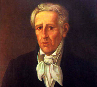
Andrés Manuel del Río

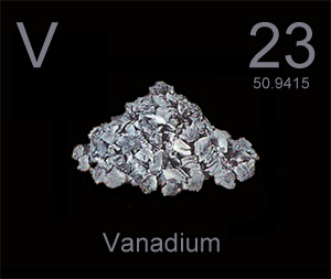
In 1801, the Mexican mineralogist Andrés Manuel del Río discovered a new element similar in nature to chromium and uranium when he studied lead ore. Its salt is red when heated in acid, so Leo named it red mud. However, it is actually vanadium.


In 1830, the Swedish chemist Nils Gabriel Sefström isolated a new element in the refining process of iron. Due to its brilliant color, he named it Vanadium under the name of the beautiful goddess Vanadis in Greek mythology. In the same year, the German chemist Friedrich Wöhler proved that Vanadium was the same element as the red element discovered by the early Andrés Manuel del Río – vanadium.

Henry Roscoe
Henry Roscoe

In 1867, the British chemist Henry Roscoe reduced the vanadium chloride (VCl3) with hydrogen to produce metal vanadium for the first time.

The origin of the name

A long time ago, a beautiful goddess named Vanadis lived in the far north. One day, a distant guest came knocking on the door. The goddess was sitting leisurely on the circle chair. She thought: If he knocked again, I would open the door. However, the knock on the door stopped and the guest left. Vanadis wants to know who this person is, why is he so lacking in self-confidence? So she opened the window and looked out. It turned out that a man named Wöhler was coming out of her yard. A few days later, the goddess heard someone knocking on the door again, and the knocking of the door didn’t stop until the goddess opened the door. This is a young and handsome man named Sefström. The goddess soon fell in love with him and gave birth to his son, vanadium.

The application history of vanadium

After discovering the metal of vanadium, people gradually learned about its properties and began to apply it to our daily lives. In 1882, a British company used vanadium-containing slag containing 1.1% vanadium to produce vanadium phosphate with an annual output of about 60 tons.

In the late 19th and early 20th centuries, Russia began to reduce iron and vanadium oxides by carbon reduction, and for the first time prepared vanadium-iron alloys (including V35% to 40%). From 1902 to 1903, Russia tested an aluminothermic method for the preparation of ferrovanadium.

At the end of the 19th century, the study also found that vanadium can significantly improve the mechanical properties of steel in steel, making vanadium widely used in industry. By the beginning of the 20th century, people began to mine vanadium.

So far, the world’s vanadium-producing ore is mainly composed of vanadium-titanium magnetite, and there are abundant resources in Russia, South Africa, China, Australia and the United States. In addition, vanadium uranium, bauxite, phosphate rock, carbonaceous shale, petroleum combustion ash, spent catalyst, etc. can also be considered as resources of vanadium.

This is a history column, aiming at introducing the discovery of different kinds of metals. If you are a metal lover or history lover, you can follow our website. For previous posts of this column please search the keyword “history”.

Please visit https://www.sputtertargets.net/ for more information.

Semiconductor industry: The importance of Anelva target

The sputtering target materials can be divided into metal target (pure metal gold, aluminumtitanium, etc.), alloy target (aluminum-scandium alloy, cobalt-aluminum alloy, aluminum-titanium alloy, etc.) and ceramic compound target (oxides, nitride, silicides, etc.) according to their different chemical compositions; when it comes to different application fields, it can be categorized into semiconductor target, planar display target, solar cell target, and other target materials. Anelva target refers to the sputtering target used in semiconductor industry.

Although the proportion of Anelva target is just about 3% among all the sputtering targets, it cannot be denied that its application in semiconductor chip market is important and irreplaceable. There are generally two kinds of Anelva target: wafer materials and packaging materials. Today we mainly focus on wafer manufacturing materials because they have relatively high technical barriers than the other.

The inner part of the semiconductor is composed of tens of thousands of meters of metal wiring, and the sputtering target material is the key consumption material for making these wiring. In other words, the Anelva target is the core of semiconductor wafer manufacturing. Since the chip is elaborate, it has high requirements for sputtering target material used in the manufacturing process. Generally, the purity of the target material is over 99.999%.

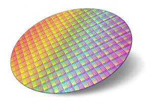
Semiconductor wafers are the basic material for manufacturing chips (as shown below). It is small but complicated. The production of wafer mainly involves 7 kinds of semiconductor materials and chemicals. The most important raw material for semiconductor integrated circuits is silicon, which is widely found in rocks and gravel in the form of silicate or silicon dioxide in nature. The manufacturing process of silicon wafers can be divided into three basic steps: silicon purification, monocrystalline silicon growth, and wafer formation. Apart from silicon, the manufacturing process of 200mm (8-inch) and below wafers is usually mainly made of aluminum, and the manufacture of 300mm (12-inch) wafer mostly uses advanced copper interconnection technology.

Semiconductor wafer

In conclusion, with more extensive use of semiconductor chips, the demand for aluminum, titanium, tantalum and copper, the four mainstream Anelva target, will also increase. There is currently no alternative to these target materials, either technically or economically, so, as I mentioned before,  they are important and irreplaceable.

Please visit https://www.sputtertargets.net/ for more information.
What should we do when the target is broken?

For most of the time, people consider the purity, and maybe the shape, of the sputtering target when they are purchasing the target materials. But one thing should not be ignored is the target bonding. Well, you think it unnecessary and costly? Then just think about what to do when your target is broken.broken target

Target bonding is necessary

Maybe you can use a copper plate to stick the broken pieces of the target and then polish the target so that the broken areas have minimum exposure to plasma. The second step is very important because the power would suddenly breakdown to zero when plasma strike to broken area of target. And obviously, the film quality will be affected if breakdown is frequent. Although it may help solve the problem when the target is broken, it is still a remedial measure. To avoid target from breaking, you need to give a target bonding service to the target. It is necessary for those brittle targets, and is not expensive compared with the losses of the broken target.

Continue reading “What should we do when the target is broken?”

PVD vs. CVD: What’s the difference?

PVD vs. CVD: What’s the difference?

In recent years, physical vapor deposition (PVD) and chemical vapor deposition (PVD) have wide applications in various industries to increase the hardness of tools and molds or apply beautiful colors to the products. Thus these two methods are considered as the most attractive surface coating technologies. Then, using the example of cutting tools, let’s make a detailed comparison between these two methods.

Definition

Physical vapor deposition (PVD) uses low-voltage, high-current arc discharge technology under vacuum conditions to evaporate the target and ionize the vaporized material and the gas, and finally make the evaporated material and its reaction deposited on the workpiece.

Continue reading “PVD vs. CVD: What’s the difference?”

Discovery and development of tungsten | History of Tungsten

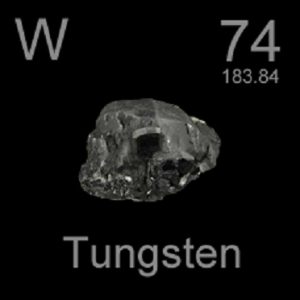
tungsten

The history of tungsten dates back to the 17th century. At that time, miners in the Erzgebirge Mountains of Saxony, Germany, noticed that some of the ore would interfere with the reduction of cassiterite and produce slag. The miners gave the mines some German nicknames: “wolfert” and “wolfrahm”.

Axel Fredrik Cronstedt

In 1758, the Swedish chemist and mineralogist Axel Fredrik Cronstedt discovered a mineral called “tungsten”, which means “heavy stone” in Swedish. He was convinced that this mineral contained an element that had not yet been discovered.


Continue reading “Discovery and development of tungsten | History of Tungsten”

What is Magnesium Fluoride?

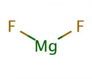
Chemical Formula of Magnesium Fluoride

SAM®Magnesium fluoride is an inorganic compound with the formula MgF2, which is a white, fluorescent crystal. It is insoluble in water and alcohol, and soluble in nitric acid. It can be used in ceramics and glass. Magnesium Fluoride is one of the lowest index infrared materials that it is transparent over a wide range of wavelengths, thus is used for optical elements in both the infrared and ultraviolet. It is resistant to thermal and mechanical shock and is twice as hard as Calcium Fluoride.

Continue reading “What is Magnesium Fluoride?”

How was niobium discovered? | History of Niobium

Last week, we talked about the discovery of Titanium, which raised many interest. So we decide to start a history column, aiming at introducing the discovery of different kinds of metals. If you are a metal lover or history lover, you can follow our website. For previous posts of this column please search the keyword “history”. So let’s get down to the point. Today SAM Sputter Targets will teach you the history lesson of Niobium.

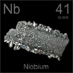
niobium hostorySAM®Niobium, often found in the minerals pyrochlore and columbite, is a silver-gray, soft and ductile rare metal with high melting point. At normal temperature, niobium does not react with air, but it can directly combine with sulfur, nitrogen and carbon at high temperatures to form NbS2, NbN and NbC. Niobium does not react with inorganic acids or alkalis, and is insoluble in aqua regia, but soluble in hydrofluoric acid. Because of its good superconductivity, high melting point, corrosion resistance and wear resistance, niobium is widely used in steel, superconducting materials, aerospace, atomic energy and other fields.

Continue reading “How was niobium discovered? | History of Niobium”

Application of molybdenum in metal smelting

Compared to metals such as titanium, aluminum and platinum, molybdenum does not seem to be as famous, but it is also a very widely used metal in our life. So in the next few weeks, SAM Sputter Targets will introduce different applications of molybdenum. If you are interested in metals, please follow us for subsequent updates. Today we will first introduce the application of molybdenum in metal smelting.

Molybdenum
Molybdenum

Steel

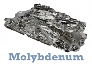
The main use of molybdenum is to produce various types of steel and alloys. The addition of molybdenum (mainly in the form of ferromolybdenum, molybdenum oxide and calcium molybdate) to a range of steels such as structural steel, spring steel, bearing steel, tool steel, stainless steel and magnetic steel can significantly improve the properties of steel. Molybdenum improves the hardenability, toughness and heat strength of steel and prevents temper brittleness. Molybdenum also improves the corrosion resistance of steel to certain media so that it does not pitting. The addition of molybdenum to the cast iron enhances the strength and wear resistance of the cast iron.

Continue reading “Application of molybdenum in metal smelting”

How was titanium discovered? | History of Titanium

Titanium historySAM®Titanium is a metal element that is known as “space metal” because of its light weight, high strength and good corrosion resistance. The most common compound of titanium is titanium dioxide, and other compounds include titanium tetrachloride and titanium trichloride. At present, titanium is widely used in aerospace, automotive, medical, marine and other fields. Its abundant reserves provide a resource base for the wide application of titanium – titanium is one of the most widely distributed and abundant elements in the earth’s crust, accounting for 0.16% of the crustal mass, ranking ninth. However, do you know how this magical element was discovered? Let SAM Sputter Targets give you a history lesson.

Continue reading “How was titanium discovered? | History of Titanium”

How is tantalum used in phones?

We have talked about the Application of Tantalum Target in Thermal Inkjet Print Head and Copper Plating before, which rises your interest on this element. However, most people think thermal inkjet print and copper plating are far away from their life, thus are difficult to understand. So today, SAM sputter targets will talk about something that EVERYONE is familiar with—your mobile phones.

tantalum

Tantalum is a very important element in the electronic industry. And it is widely used in all kinds of electronic devices, such as phones and computers. The main use of tantalum materials in electronic products comes in the creation of tantalum capacitor. Tantalum capacitors have their unique advantages over other capacitors. They do not use electrolytes like ordinary electrolytic capacitors, making them ideal for operation at high temperatures. Solid tantalum capacitors have excellent electronic properties, wide operating temperature range, various forms and excellent volumetric efficiency.

Continue reading “How is tantalum used in phones?”