Lithium Battery Technology-An Overview

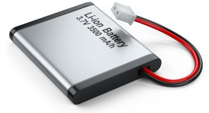
What is a lithium battery?

Contrary to some beliefs, lithium batteries are not exclusively composed of metallic lithium. Instead, they encompass a broad category of batteries that can be generally divided into two types: lithium metal batteries and lithium-ion batteries. Typically, the term “lithium battery” refers to batteries that use a lithium metal or lithium alloy as the anode and a non-aqueous electrolyte.

One of the most commonly used lithium-based chemicals in renewable energy applications is lithium iron phosphate (LiFePO4). LiFePO4 batteries are known for their high safety standards, excellent thermal stability, high rated current capacity, and long cycle life. These characteristics make them suitable for various applications, including electric vehicles, energy storage systems, and portable electronics.

Lithium battery2

Advantages

Lithium batteries offer several advantages over traditional batteries like lead-acid, nickel-chrome, and nickel-hydrogen batteries:

  1. Environmental Impact: Lithium batteries do not contain harmful heavy metals such as lead, mercury, or cadmium, making them more environmentally friendly. Their electrolytes are typically organic solvents and lithium salts, which are mostly non-toxic or low-toxic, resulting in relatively low pollution.
  2. Safety: Lithium batteries do not pose a risk of exposure to corrosive electrolytes like sulfuric acid or potassium hydroxide. They generally do not present an explosion hazard even when stored in confined spaces, and their well-designed systems eliminate the need for active cooling or ventilation.
  3. Longevity: Lithium batteries have an exceptionally long cycle life, with some manufacturers guaranteeing up to 10,000 cycles. This long lifespan makes them a cost-effective solution in the long run.
  4. Performance: Lithium batteries provide high energy density, allowing for compact and lightweight battery designs. They also offer high efficiency, quick charging times, and a wide operating temperature range, making them suitable for various demanding applications.
  5. Maintenance: Unlike some traditional batteries, lithium batteries require minimal maintenance, which reduces the total cost of ownership.

Application

The advent of microelectronics technology in the twentieth century has led to an increased demand for miniaturized devices with high-performance power supplies. As a result, lithium batteries have become widely used in various fields:

1. Semiconductor Manufacturing:
  • Wafer Processing: Utilized in semiconductor wafer processing equipment for applications such as epitaxy, chemical vapor deposition (CVD), and physical vapor deposition (PVD).
  • Test Equipment: Employed in test and measurement equipment for semiconductor devices.
2. Medical and Laboratory Equipment:
  • DNA Amplification: Used in PCR (Polymerase Chain Reaction) devices for DNA amplification, where precise temperature control is essential.
  • Analytical Instruments: Integrated into analytical instruments requiring high-temperature operation, such as mass spectrometers and chromatography equipment.
3. Aerospace and Defense:
  • Thermal Management: Utilized in thermal management systems for avionics and other high-performance electronic systems.
4. Industrial Heating:
  • Plastic Welding: Used in plastic welding equipment that requires high temperatures for precise welding operations.
  • Heating Plates and Hot Plates: Employed in heating plates and hot plates for various industrial processes.
5. Optoelectronics:
  • LED Manufacturing: Used in the production of LEDs, where high temperatures and precise control are necessary.
  • Laser Diodes: Integrated into laser diode assemblies for efficient thermal management.
6. Consumer Electronics:
  • Mobile Devices: Lithium-ion batteries power a wide range of mobile devices, including smartphones, tablets, and laptops, due to their compact size and high energy density.
  • Wearable Technology: Used in smartwatches, fitness trackers, and other wearable devices, providing reliable power in a small form factor.
7. Electric Vehicles (EVs):
  • Battery Packs: Lithium-ion batteries are the preferred choice for electric vehicles due to their high energy density, long cycle life, and ability to provide the necessary power for vehicle propulsion.
  • Charging Infrastructure: Supporting fast-charging stations and home charging units, facilitating the widespread adoption of electric vehicles.
8. Renewable Energy Storage:
  • Grid Storage: Lithium batteries are used in large-scale energy storage systems to store electricity generated from renewable sources like solar and wind, ensuring a stable and reliable energy supply.
  • Residential Energy Storage: Used in home energy storage systems, enabling homeowners to store excess solar energy for use during peak demand periods or power outages.

Read more: Understanding Lithium Selenide: Uses and Importance of Sputtering Targets

About Stanford Advanced Materials (SAM)

Stanford Advanced Materials (SAM) Corporation is a global supplier of various sputtering targets, including metals, alloys, oxides, and ceramic materials. We offer high-purity lithium metal, sputtering targets, and evaporation materials. For more information, please visit our website at SAM Sputter Targets.

What is Extreme High Speed Laser Material Deposition(EHLA)?

The German research institute Fraunhofer Institute for Laser Technology has developed a groundbreaking metal part coating process called Extreme High Speed Laser Material Deposition (EHLA). This innovative technique promises to revolutionize the way metal coatings are applied, offering significant improvements in efficiency, speed, and environmental impact.

How EHLA Works

EHLA involves using a laser to create a molten pool on the surface of a component. A precise amount of metal powder is then added to this pool. Unlike traditional laser deposition processes, the powder in EHLA melts completely before it is deposited on the part’s surface. This ensures a thin, uniform coating that is both durable and resource-efficient. Remarkably, EHLA introduces approximately 90% of the material into the desired area, compared to just 50% in other methods.

Extreme High Speed Laser Material Deposition

Speed and Efficiency

The standout feature of EHLA is its exceptional speed. Coating processes using EHLA can be performed at speeds 100 to 250 times faster than conventional laser material deposition techniques. This rapid application rate drastically reduces processing time, making EHLA an attractive option for high-volume production environments.

Heat Sensitivity and Versatility

One of the key advantages of EHLA is its minimal heat generation during processing. This makes it ideal for coating heat-sensitive components without causing thermal damage. Additionally, EHLA is capable of tandem coating processing, which allows for the application of multiple layers or different materials in a single operation. This versatility opens up new possibilities for advanced coatings that can enhance the performance and longevity of metal parts.

Environmental Benefits

EHLA stands out for its environmental friendliness. The process eliminates the need for chromium, a chemical commonly used in traditional coating processes that is harmful to the environment. EHLA uses no hazardous chemicals, making it a safer and more sustainable option. Moreover, the coating adheres to the substrate in a material-locking manner, preventing peeling and ensuring a long-lasting bond.

Applications and Future Prospects

Researchers are excited about the potential applications of EHLA. The process is effective in protecting metal parts from corrosion and wear, extending the life cycle of products. It is compatible with various coatings, including iron, nickel, and cobalt-based alloys, making it suitable for a wide range of industrial applications.

With its impressive speed, efficiency, and environmental benefits, EHLA presents a promising future for metal coating technologies. It offers a sustainable solution that not only enhances the performance of metal parts but also reduces resource consumption and environmental impact.

About Stanford Advanced Materials

Stanford Advanced Materials (SAM) Corporation is a global supplier of various sputtering targets such as metals, alloys, oxides, and ceramic materials. If you are interested in learning more about EHLA or our range of products, please visit our website at SAM Sputter Targets for more information.

Aluminum-Doped Zinc Oxide: Applications

Introduction

Aluminum-doped zinc oxide (AZO) is a transparent conductive oxide (TCO) that has garnered significant attention for its impressive combination of electrical conductivity and optical transparency. These properties make AZO a highly versatile material, finding applications in various fields ranging from renewable energy to advanced electronics. This article delves into the numerous applications of AZO, highlighting its critical role in modern technology. Notably, Stanford Advanced Materials is a key supplier of high-quality AZO thin-film coatings.

Solar Cells

One of the most prominent applications of AZO is in the production of solar cells. AZO serves as a transparent conductive electrode, a crucial component that allows light to reach the active layer of the solar cell while conducting the generated electrical current efficiently. Its high transparency ensures minimal loss of light, while its low resistivity facilitates effective current collection, enhancing the overall efficiency of the solar cells.

Polycrystalline Silicon Solar Cells
Ogunshile, Emmanuel. (2017). An Investigation into the Use of Hybrid Solar Power and Cloud Service Solutions for 24/7 Computing. 743-754. 10.5220/0006380007430754.

Key Points:

  • Transparent Electrode: Allows light to reach the active layer of the solar cell.
  • Efficient Current Collection: Low resistivity ensures minimal electrical losses.

Flat-Panel Displays

AZO is widely used in the manufacture of flat-panel displays, including LCDs and OLEDs. In these applications, AZO functions as a transparent conductive layer that forms part of the display’s electrode structure. Its high optical transparency ensures clear and vibrant displays, while its electrical conductivity supports the operation of the display’s pixels.

Key Points:

  • High Optical Transparency: Ensures clear and vibrant displays.
  • Conductive Layer: Supports the operation of the display’s pixels.

Touch Screens

Touch screens in smartphones, tablets, and other electronic devices rely on transparent conductive materials to detect touch inputs. AZO, with its excellent transparency and conductivity, is an ideal material for touch screen applications. It allows for precise touch detection while maintaining the screen’s clarity and responsiveness.

Key Points:

  • Precise Touch Detection: Supports accurate and responsive touch screens.
  • Maintains Screen Clarity: High transparency ensures clear display quality.

Smart Windows

Smart windows, also known as electrochromic windows, can change their transparency in response to an applied voltage. AZO is used as a transparent electrode in these windows, playing a critical role in their ability to modulate light transmission. This application is particularly valuable in energy-efficient building designs, where smart windows help regulate indoor temperature and lighting.

Key Points:

  • Modulates Light Transmission: Allows smart windows to change transparency.
  • Energy Efficiency: Contributes to temperature and lighting regulation in buildings.

Light-Emitting Diodes (LEDs)

In LED technology, AZO is used as a transparent electrode, particularly in ultraviolet and visible light LEDs. Its high conductivity and transparency enhance the efficiency of LEDs by ensuring effective current injection and minimal light absorption. This application is essential for creating bright and energy-efficient lighting solutions.

Key Points:

  • Enhances LED Efficiency: Effective current injection and minimal light absorption.
  • Bright and Energy-Efficient Lighting: Supports the development of advanced LED technologies.

Thin-Film Transistors (TFTs)

Thin-film transistors are critical components in a variety of electronic devices, including displays and sensors. AZO is employed as a channel layer or electrode material in TFTs due to its excellent electrical properties. Its use in TFTs helps improve the performance and reliability of electronic circuits.

Key Points:

  • Improves Performance: Enhances the efficiency and reliability of electronic circuits.
  • Versatile Component: Used in displays, sensors, and other electronic devices.

Photodetectors

Photodetectors, which are used to detect light and convert it into electrical signals, benefit from the use of AZO. Its high transparency and conductivity make it an ideal material for the transparent electrodes in photodetectors, improving their sensitivity and response time. This application is vital in various fields, including medical imaging, environmental monitoring, and security systems.

Key Points:

  • Improves Sensitivity: Enhances the detection capabilities of photodetectors.
  • Fast Response Time: Ensures quick and accurate light detection.

Conclusion

Aluminum-doped zinc oxide (AZO) is a versatile material with a wide range of applications in modern technology. From solar cells and flat-panel displays to touch screens and smart windows, AZO’s unique properties of high electrical conductivity and optical transparency make it an indispensable component in many advanced electronic devices. As technology continues to evolve, the role of AZO in improving efficiency, performance, and functionality in various applications is set to expand, driving innovations and enhancing the capabilities of future technologies. Stanford Advanced Materials, a leading supplier of high-quality AZO thin-film coatings, plays a crucial role in supporting these advancements.

Indium Phosphide Wafer Applications: Revolutionizing Technology Across Fields

Indium phosphide (InP) wafers are at the forefront of technological innovation, serving as a foundational element in several cutting-edge applications. Known for their excellent electronic and optoelectronic properties, InP wafers are instrumental in advancing industries from automotive to telecommunications and energy. Here, we explore the diverse applications of Indium phosphide wafers, demonstrating their crucial role in modern technology.

Optoelectronic Components

Indium phosphide wafers are pivotal in the development of optoelectronic components, particularly in the realm of terahertz technology. This application is incredibly beneficial in ultra-sensitive spectroscopic analyzers used to measure the thickness of polymers and detect multilayer coatings. These capabilities are extensively utilized in the automotive industry, enhancing the precision and reliability of vehicle manufacturing processes.

High-Speed Electronics

In the domain of electronics, InP wafers are synonymous with speed and efficiency. They are essential in creating the fastest semiconductor devices currently available. Devices such as High Electron Mobility Transistors (HEMTs) and Heterostructure Bipolar Transistors (HBTs) rely on InP for their operations. The high-speed capabilities of microelectronics developed on InP make them indispensable in sectors where rapid data processing and transmission are required, such as telecommunications and advanced computing.

Photovoltaics

Indium phosphide also plays a transformative role in the energy sector, particularly in solar power technology. Photovoltaic cells made with InP substrates are among the most efficient, with performance capabilities reaching up to 46% efficiency. The key to this high efficiency is InP’s optimal bandgap combination, which allows for effective conversion of solar radiation into electrical energy. The unique lattice constant of InP is ideal for growing low bandgap materials with high crystalline quality, critical for high-performance solar cells.

Photonic Integrated Circuits

Beyond these applications, InP is also a crucial material in the manufacturing of photonic integrated circuits (PICs). These circuits integrate active laser generation, amplification, control, and detection, all on a single chip. The properties of InP make it excellent for these functions, which are essential in communication and sensing technologies. Photonic integrated circuits based on InP are fundamental in pushing the boundaries of optical communication, including fiber optics and laser technologies.

Unlocking the Terahertz Range

Indium phosphide-based components have the unique ability to unlock the terahertz zone of the electromagnetic spectrum, which lies between infrared and microwaves. This part of the spectrum is significant for its hybrid properties, combining high-frequency and high-optical qualities, which are promising for future applications in imaging, sensing, and wireless communications.

Conclusion

The versatility and superior properties of Indium phosphide wafers make them a cornerstone in multiple high-tech applications across various industries. From enhancing the efficiency of solar panels to enabling high-speed electronics and advancing optical communications, InP wafers continue to be integral to the evolution of technology. As research progresses and the potential applications of this material expand, InP may soon play a part in even more revolutionary technologies.

For high-quality InP wafer or other crystal substrates, please visit https://www.sputtertargets.net/product-category/crystal-substrates/.