Spherical Nickel Powder vs. Traditional Nickel Powder: A Comparative Analysis

In the realm of metal powders, nickel holds a significant place due to its versatility and wide-ranging applications. Recently, the emergence of spherical nickel powder has sparked considerable interest, prompting comparisons with traditional nickel powder. In this article, we delve into the distinctions between these two forms of nickel powder and explore the scenarios where each shines.

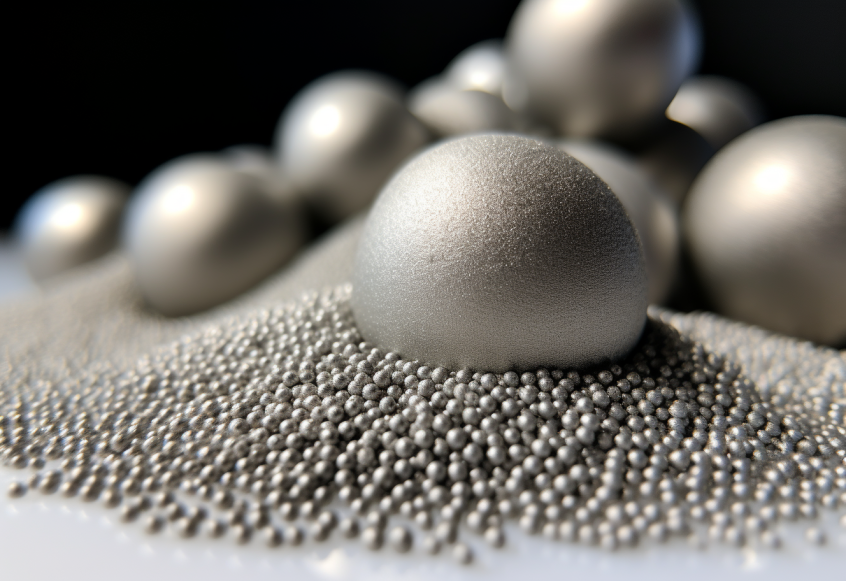
Particle Morphology: Spherical vs. Irregular

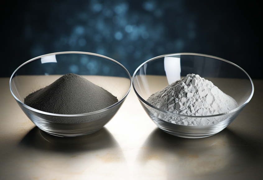
The most noticeable difference between spherical nickel powder and traditional nickel powder lies in their particle morphology. Spherical nickel powder is characterized by its uniform, spherical particle shape, while traditional nickel powder consists of irregularly shaped particles. This distinction plays a pivotal role in various aspects of their performance and applications.

Flowability and Packing Density

Spherical nickel powder’s uniform shape offers enhanced flowability and packing density. During manufacturing processes like additive manufacturing, the particles flow smoothly and evenly, resulting in higher material utilization and reduced powder wastage. In contrast, traditional nickel powder’s irregular particles can lead to uneven flow, resulting in challenges during processing and decreased packing density.

Porosity and Structural Integrity

The shape of nickel powder particles directly impacts the porosity and structural integrity of the final product. Spherical nickel powder’s uniform packing leads to reduced porosity and improved mechanical properties. This makes it an excellent choice for applications where high strength and dimensional accuracy are paramount. Traditional nickel powder, due to its irregular particles, can result in higher porosity levels and reduced structural integrity.

Surface Quality and Finish

Spherical nickel powder’s uniform particle size distribution contributes to smoother surfaces and finer finishes in products. This is particularly crucial in industries where aesthetics and surface quality play a significant role. On the other hand, traditional nickel powder’s irregular particles can lead to rougher surfaces and increased post-processing requirements.

Applications and Industries

The choice between spherical nickel powder and traditional nickel powder largely depends on the specific application and industry requirements. Spherical nickel powder’s advantages make it a prime candidate for additive manufacturing, aerospace components, and electronics, where precision and performance are essential. Traditional nickel powder remains relevant in applications that don’t require the same level of uniformity and performance, such as certain types of coatings and metallurgical processes.

The Road Ahead

Both spherical nickel powder and traditional nickel powder have their distinct roles in the realm of material science and manufacturing. As industries continue to innovate and push boundaries, the choice between these two forms of nickel powder will depend on the specific performance criteria, design requirements, and production methods.

In conclusion, the comparison between spherical nickel powder and traditional nickel powder underscores the critical role that particle morphology plays in material performance and applications. While each form has its advantages, the choice ultimately depends on the unique demands of the project and the desired outcome.

For more information about spherical nickel powder or spherical powder for 3d printing, please visit https://www.sputtertargets.net/.

Advantages of Using Spherical Nickel Powder in Additive Manufacturing

Additive manufacturing, commonly known as 3D printing, has ushered in a new era of manufacturing possibilities. Among the various materials used in this innovative technology, spherical nickel powder stands out for its remarkable properties and advantages. In this article, we delve into the world of additive manufacturing and explore the reasons why spherical nickel powder is becoming a game-changer in this field.

The Unique Attributes of Spherical Nickel Powder

Spherical nickel powder possesses a distinct advantage over traditional nickel powder due to its shape and size uniformity. The spherical shape of the particles ensures consistent flowability and improved packing density during the printing process. This leads to enhanced layer-to-layer adhesion and reduced porosity in the printed objects, resulting in parts with higher mechanical strength and improved structural integrity.

Tailoring Material Properties

Additive manufacturing allows engineers and designers to create intricate and complex geometries that were once thought impossible. Spherical nickel powder contributes to this capability by enabling the production of fine, intricate structures with high surface quality. Its uniform particle size distribution ensures an even deposition of layers, leading to smooth surfaces and accurate dimensional accuracy. Moreover, the material’s excellent thermal and electrical conductivity make it ideal for applications requiring heat dissipation and electrical connectivity.

Advancements in Functional Parts

The aerospace and automotive industries are leveraging spherical nickel powder’s unique properties to produce functional parts with exceptional performance characteristics. In aerospace, components like engine turbines and fuel nozzles benefit from the material’s ability to withstand high temperatures and corrosive environments. Similarly, in the automotive sector, the use of spherical nickel powder is contributing to the development of lightweight, high-strength parts that enhance fuel efficiency and overall vehicle performance.

The Path to Sustainability

As industries increasingly focus on sustainability, the role of materials like spherical nickel powder becomes crucial. Its efficient use in additive manufacturing results in minimal material wastage, making it an environmentally friendly choice. Additionally, the potential for recycling and reusing powder not used during printing further reduces material consumption and waste generation.

Challenges and Future Directions

While spherical nickel powder holds immense promise, challenges such as powder handling and production costs remain. Researchers and manufacturers are actively working to overcome these hurdles, paving the way for broader adoption of this advanced material. As additive manufacturing continues to evolve, the synergy between technology and material innovation will likely lead to breakthroughs in both performance and affordability.

In conclusion, spherical nickel powder is transforming the additive manufacturing landscape by offering unparalleled advantages in terms of material properties, design flexibility, and sustainability. Its role in producing functional parts for industries ranging from aerospace to automotive underscores its importance in shaping the future of manufacturing.

For more information about spherical nickel powder or spherical powder for 3d printing, please visit https://www.sputtertargets.net/.

Zinc Oxide Thin Films in Nanotechnology: Synthesis and Applications

Introduction

Zinc oxide (ZnO) is a wide-bandgap semiconductor with diverse properties that have garnered significant attention in nanotechnology research. The synthesis of zinc oxide thin films using sputtering targets has opened up new possibilities for various nanoscale applications. This article explores the synthesis process of ZnO thin films through sputtering and delves into their emerging applications in the field of nanotechnology.

Synthesis of Zinc Oxide Thin Films using Sputtering Targets

Sputtering is a popular thin film deposition technique that involves bombarding a target material with high-energy ions to release atoms or molecules, which then condense on a substrate to form a thin film. The sputtering process for zinc oxide thin films is typically carried out in a vacuum chamber, where an argon plasma is used to dislodge zinc oxide atoms from a sputtering target. The sputtered atoms travel through the vacuum and deposit onto a substrate, forming a thin film.

One of the main advantages of sputtering is the ability to precisely control the thickness and composition of the thin film. This level of control allows researchers to tailor the properties of zinc oxide thin films for specific nanotechnology applications.

Properties of Zinc Oxide Thin Films

Zinc oxide thin films possess several unique properties that make them highly attractive for nanoscale applications. Firstly, ZnO is a wide-bandgap semiconductor, making it suitable for optoelectronic devices such as light-emitting diodes (LEDs) and photodetectors. The wide bandgap allows ZnO thin films to emit and detect light in the ultraviolet region, which is essential for various optical and sensing applications.

Additionally, zinc oxide exhibits excellent piezoelectric properties, meaning it can convert mechanical energy into electrical signals and vice versa. This property has opened up opportunities for ZnO thin films in nanoelectromechanical systems (NEMS) and sensors.

Applications of Zinc Oxide Thin Films in Nanotechnology:

  1. Nanosensors: Zinc oxide thin films are used as sensitive layers in gas sensors and biosensors due to their high surface area and excellent sensing properties. They have been employed in detecting gases such as ammonia, carbon monoxide, and hydrogen, making them valuable for environmental monitoring and medical diagnostics.
  2. Nanodevices: ZnO thin films find applications in the development of nanodevices like field-effect transistors (FETs) and nanogenerators. Their exceptional piezoelectric characteristics make them ideal for energy harvesting applications.
  3. Nanophotonics: Zinc oxide thin films are used in the fabrication of nanophotonic devices, including waveguides and microcavities. Their ability to emit and manipulate light at the nanoscale level makes them essential in advanced optical communication systems.
  4. Nanocoatings: ZnO thin films serve as protective nanocoatings for various surfaces, providing enhanced resistance to environmental factors like UV radiation and corrosion.

Conclusion

Zinc oxide thin films synthesized using ZnO sputtering targets have emerged as a key player in the field of nanotechnology. Their versatile properties and precise synthesis make them ideal for a wide range of nanoscale applications. As researchers continue to explore the unique properties of ZnO thin films, we can expect to see further advancements in nanotechnology, leading to innovative devices and technologies that address various global challenges.

For more information about ZnO sputtering target or other thin film coating materials, please visit https://www.sputtertargets.net/.

Molybdenum Targets in Semiconductor Manufacturing

Introduction

Semiconductor manufacturing is at the heart of modern technology, driving advancements in electronics, telecommunications, and computing. Key to this process is the use of specialized materials and techniques, with molybdenum targets playing a crucial role in thin film deposition. This article delves into the significance of molybdenum targets in semiconductor manufacturing, exploring their applications and advantages in enabling the creation of high-performance electronic devices.

Molybdenum Targets and Thin Film Deposition

Thin film deposition is a fundamental process in semiconductor manufacturing, where thin layers of material are precisely deposited onto a substrate to form integrated circuits and other electronic components. Molybdenum targets, typically in the form of sputtering targets, are vital to this process due to their exceptional material properties. Molybdenum is a refractory metal, offering high melting points and excellent thermal stability, making it suitable for use in demanding high-temperature environments during thin film deposition.

Sputtering is the primary technique employed for depositing thin films using molybdenum targets. In this process, molybdenum atoms are sputtered from the target’s surface through ion bombardment and subsequently deposited onto the substrate. The precise control of this deposition allows for the creation of uniform and well-adhered thin films with precise thicknesses, critical for the functionality of semiconductor devices.

Applications in Semiconductor Devices

Molybdenum targets find widespread use in semiconductor manufacturing for various applications. One of the primary applications is in the creation of gate electrodes in metal-oxide-semiconductor field-effect transistors (MOSFETs). MOSFETs are essential components of integrated circuits, controlling the flow of electrical current and enabling the amplification of signals in electronic devices. The high thermal and electrical conductivity of molybdenum makes it an ideal choice for gate electrodes, ensuring efficient device performance.

Additionally, molybdenum targets are used in the fabrication of interconnects, which serve as conductive pathways between different components on the semiconductor device. The high purity and uniformity of molybdenum thin films are critical for achieving low electrical resistance in interconnects, minimizing power losses and improving the overall efficiency of electronic devices.

Advantages of Molybdenum Targets

Several key advantages make molybdenum targets stand out in semiconductor manufacturing:

  1. Thermal Stability: Molybdenum targets can withstand high temperatures, ensuring stability during the deposition process. This is particularly important for high-temperature processing steps in semiconductor manufacturing.
  2. High Purity: The exceptional purity levels of molybdenum targets enable the deposition of clean and contamination-free thin films, resulting in reliable semiconductor devices with consistent performance.
  3. Uniformity: Molybdenum targets facilitate the creation of uniform thin films, ensuring consistent device characteristics across a wafer and improving the overall yield of the manufacturing process.
  4. Compatibility: Molybdenum targets are compatible with various deposition techniques, offering flexibility in thin film deposition processes for different semiconductor applications.

Conclusion

In conclusion, molybdenum targets play a critical role in semiconductor manufacturing by enabling precise thin film deposition. Their exceptional thermal stability, high purity, and uniformity make them indispensable for the creation of high-performance semiconductor devices. From MOSFET gate electrodes to interconnects, molybdenum targets contribute to the advancement of modern technology, ensuring reliable and efficient electronic devices that power our digital world. As semiconductor technology continues to evolve, molybdenum targets will remain at the forefront, driving innovation and shaping the future of electronics.

For more information about molybdnem sputtering target or other target materials, please visit https://www.sputtertargets.net/.