Optical Coating: Anti-wear films (hard coating film)

As a raw material for the deposition of hard coatings by PVD technology, the target will directly affect the physical and mechanical properties of the hard coating films. Therefore, the selection of good sputtering targets for coating preparation is of great practical significance.

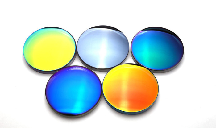
Spectacle lenses made of inorganic materials or organic materials can cause scratches on the surface of the lens due to friction with dust or gravel (silicon oxide) during daily use. Compared with glass sheets, organic materials have lower hardness and are more likely to cause scratches. Through the microscope, we can observe that the scratches on the surface of the lens are mainly divided into two types: one is because the scratches generated by the gravel are shallow and small, and the wearer is not easy to detect; the other is the scratch caused by the larger gravel, which is deep and peripherally rough, and will affect people’s vision if it is in the central area. In order to improve the anti-wear of optical lenses, people began to study optical coatings to produce anti-wear films.

glass-lens-scratches-optical-coating

Technical Development

First generation anti-wear film technology

Anti-wear films began in the early 1970s when it was thought that glass lenses were not easy to wear because of their high hardness, while organic lenses were easy to wear because they are too soft. Therefore, the quartz material is plated on the surface of the organic lens under vacuum to form a very hard anti-wear film. However, due to the mismatch between the thermal expansion coefficient and the substrate-based material, the film is easy to take off and the film layer is brittle, thus the anti-wear effect is not ideal.

Second generation anti-wear film technology

After the 1980s, researchers theoretically found that the mechanism of wear is not only related to hardness, but also related to the dual characteristics of “hardness/deformation” of the film material, that is, some materials have higher hardness but less deformation, while some materials have lower hardness but greater deformation. The second generation of anti-wear film technology is to apply a high hardness and less brittle material to the surface of the organic lens by the immersion process.

Third generation anti-wear film technology

The third generation of anti-wear film technology was developed after the 1990s, mainly to solve the problem of wear resistance after the organic lens is coated with anti-reflection film. Since the hardness of the organic lens substrate and the hardness of the anti-reflection film layer are very different, the new theory suggests that an anti-wear film layer is required between the two layers, so that the lens are not easy to be scratched. The hardness of the third-generation anti-wear film material is between the hardness of the anti-reflection film and the lens base, and the friction coefficient is low and is not easily cracked.
optical coating

Hard coating film preparation technology

Physical vapor deposition is the mainstream technology of hard coating materials preparation. The main methods are sputtering, such as magnetron sputtering; and cathode arc evaporation, such as multi-arc ion plating.

Sputter Coating

Sputtering uses ions generated by an ion source (generally Ar ions), and accelerates them into a high-speed. The high-energy ion beam in a vacuum electric field bombards the surface of the sputtering target, and kinetic energy exchange between ions and target atoms. When the ion energy is sufficient, atoms on the surface of the sputtering target will leave the target and deposit on the surface of the substrate to form a thin film.

Cathodic arc evaporation

Cathodic arc evaporation is a PVD deposition method that uses arc evaporation electrode material as a deposition source. The low-voltage, high-current electron beam forms an arc on the surface of the material. When the arc moves on the surface of the target, the high current forms a local high temperature, which causes the surface of the metal ion evaporation material on the target surface to form a plasma. After that, a high-speed high-energy ion current is obtained by the electric field, and a film of the coating material is deposited on the surface of the substrate.

As a raw material for the deposition of hard coatings by PVD technology, the target will directly affect the physical and mechanical properties of the hard coating films. Therefore, the selection of good sputtering targets for coating preparation is of great practical significance.

Please visit https://www.sputtertargets.net/ for more information.

A short analysis of sputtering targets for semiconductor application

Semiconductors have high requirements for the quality and purity of the sputtering materials, which explains why the price of anelva  targets is relatively high.

Undoubtedly, sputtering targets are the most important raw materials in current semiconductor manufacturing processes. Their quality and purity play a key role in the subsequent production quality of the semiconductor industry chain. And anelva targets refer to those sputtering targets used in the semiconductor industry.

Application requirements

Semiconductors have high requirements for the quality and purity of the sputtering materials, which explains why the price of anelva  targets is relatively high. In the semiconductor manufacturing process, if the impurity content of the sputtering target is too high, the formed film cannot achieve the required electrical properties, and it is liable to cause short circuit or damage of the circuit, which will seriously affect the performance of the film.

Therefore, when purchasing semiconductor targets, be sure to find a reliable sputtering targets manufacturers for high-quality & high-purity sputtering targets.

blue computer circuit board closeup , semiconductor industry

Market Size

With the rapid development of terminal applications such as consumer electronics, the market sales of high-purity sputtering targets are expanding.

According to statistics, in 2015, the global high-purity sputtering target market sales reached 9.48 billion US dollars, of which, the semiconductor sputtering target market sales of 1.14 billion US dollars. It is estimated that in the next five years, the market size of the world’s sputtering targets will exceed 16 billion US dollars, and the CAGR (Compound Annual Growth rate) of the high-purity sputtering target market will reach 13%.

According to statistics from WSTS (World Semiconductor Trade Statistics), the global target market is expected to grow at the same rate as 2017 (13%). In 2016, the global sputtering target market capacity was US$11.36 billion, an increase of 20% compared to US$9.48 billion in 2015. It can be inferred that the market size of the global high-purity sputtering target in 2018 is about 14.5 billion US dollars.

Stanford Advanced Materials (SAM) Corporation is a global supplier of sputtering targets such as metals, alloys, oxides and ceramic materials, which are widely used in multiple industries. Please visit https://www.sputtertargets.net/ for more information.

What is Target Poisoning in Sputtering Deposition?

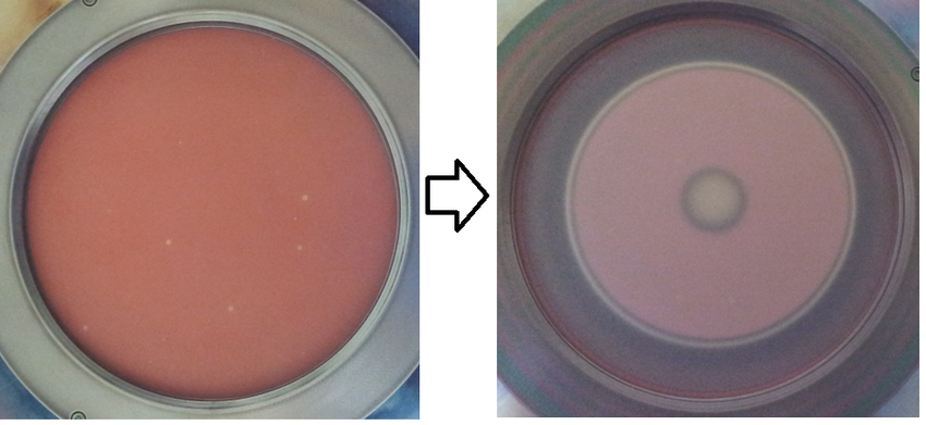
At some stage in the sputtering deposition, positive ions are continuously amassed on the surface of the sputtering target. Due to the fact that those fantastic ions aren’t neutralized, the negative bias of the target surface gradually decreases, and progressively the normal operation can not be completed. This is the target poisoning phenomenon.

The word “poisoning” is normally used to describe the poisoning as a result of the consumption of positive toxic substances via dwelling organisms. However, have you ever heard of target poisoning? Do you already know what it is?

Definition

Despite the fact that the same word is used for “poisoning”, the meaning of target poisoning and human poisoning is completely different. At some stage in the sputtering deposition, positive ions are continuously amassed on the surface of the sputtering target. Due to the fact that those fantastic ions aren’t neutralized, the negative bias of the target surface gradually decreases, and progressively the normal operation can not be completed. This is the target poisoning phenomenon.

target poisoning
target poisoning

Reasons

Target poisoning does not always occur. It is associated with various reasons, of which the following factors are the most significant:

1 There is air leak or water leakage occurs in the vacuum chamber; There are volatile components in the vacuum chamber; The vacuum chamber is not filled with argon, but mixed with air or other gases.

2 The impurity component reacts with the sputtering material to form certain substances, which cover the surface of the sputtering target and affect the film formation speed.

3 There is a change in secondary electron emission, which results in a change of the discharge impedance. Consequently, at the same discharge power, the current and voltage can change substantially as reactive gas is introduced.

Solutions

Luckily, as I mentioned before, the poisoning the the target surface does not always occur, and it can be prevented by the following methods:

1 Ensure that the vacuum chamber is not leaking; Clean the inside of the vacuum chamber regularly to remove volatile components.

2 Irradiate the sputtering target with a medium source or Radio Frequancy (RF) source for one to two hours.

3 If target poisoning occurs, the sputtering target should be removed and be polished with sandpaper.

Please visit https://www.sputtertargets.net/ for more information.
How was aluminum discovered?| History of Aluminum

AluminumDiscovery

Humphry Davy
Humphry Davy

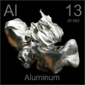
Compared with other metal elements we discussed about before, Aluminum is discovered much later. In 1808, the British chemist Sir Humphry Davy confirmed the existence of alum and named the substance to Alumium (later changed to Aluminum).

In 1825, Danish chemist and physicist Hans Christian Ørsted began experimenting about aluminum extraction. However, it was not until 1827 that Friedrich Wöhler reduced the molten anhydrous aluminum chloride with potassium metal to obtain a purer metallic aluminum element.

As precious as gold

However, as Wöhler’s method could not yield great quantities of aluminium, the metal remained rare; its cost exceeded that of gold. It is for this reason that aluminum was in a high position at that time. It is said that at a banquet, the French emperor Napoleon used aluminum knives and forks alone, while others used silver tableware. Also, the king of Thailand once used an aluminum bracelet.

Mass production

Charles Martin Hall
Charles Martin Hall

In 1886, French engineer Paul Héroult and American engineer Charles Martin Hall, respectively, independently electrolyzed a mixture of molten bauxite and cryolite to produce metal aluminum, which laid the foundation for large-scale production of aluminum in the future. Since then, the status of aluminum has changed completely, mainly in two aspects: first, it is mass-produced and is no longer regarded as a precious metal; the mass production of aluminum in industrial and domestic applications has gradually replaced the use of other metals such as steel and copper in many fields.

Application Prospect

At present, the aluminum industry has problems such as overcapacity and insufficient utilization, so the development prospects of the aluminum industry in the short term are not optimistic.

However, due to the abundant reserves of aluminum in the earth’s crust and the advantages over other metal elements, aluminum will have extremely broad application prospects in the future. For example, automakers are currently exploring the use of large-area aluminum alloy instead of steel to make the car lighter.

With the advancement of technology, aluminum alloy products will not only grow rapidly in traditional applications such as aerospace, transportation, electronic power, and construction, but will also grow rapidly in other new fields.


This is a history column of SAM Sputter Target, aiming at introducing the history of different metals. If you are a metal lover or history lover, you can follow our website. For previous posts of this column please search the keyword “history”.


Please visit https://www.sputtertargets.net/ for more information.
Basic Requirements of High Quality Titanium Sputtering Target

Purity

Purity is one of the main performance indicators of sputtering targets because it has a great influence on the performance of the film. Taking titanium target as an example, the higher the purity is, the better the corrosion resistance and electrical and optical properties of the sputtered film are. However, in practical applications, the purity requirements of the sputtering targets are not the same. Generally, the purity requirements of industrial targets are not high, but the sputter targets for semiconductors, display devices have very strict requirements–the purity requirements of magnetic film targets are generally 99.9% or more, and the purity of indium oxide and tin oxide in ITO targets is required to be not less than 99.99%.

Continue reading “Basic Requirements of High Quality Titanium Sputtering Target”

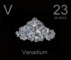
Discovery and application of vanadium | History of Vanadium

Discovery of vanadium

Andrés Manuel del Río

In 1801, the Mexican mineralogist Andrés Manuel del Río discovered a new element similar in nature to chromium and uranium when he studied lead ore. Its salt is red when heated in acid, so Leo named it red mud. However, it is actually vanadium.


In 1830, the Swedish chemist Nils Gabriel Sefström isolated a new element in the refining process of iron. Due to its brilliant color, he named it Vanadium under the name of the beautiful goddess Vanadis in Greek mythology. In the same year, the German chemist Friedrich Wöhler proved that Vanadium was the same element as the red element discovered by the early Andrés Manuel del Río – vanadium.

Henry Roscoe
Henry Roscoe

In 1867, the British chemist Henry Roscoe reduced the vanadium chloride (VCl3) with hydrogen to produce metal vanadium for the first time.

The origin of the name

A long time ago, a beautiful goddess named Vanadis lived in the far north. One day, a distant guest came knocking on the door. The goddess was sitting leisurely on the circle chair. She thought: If he knocked again, I would open the door. However, the knock on the door stopped and the guest left. Vanadis wants to know who this person is, why is he so lacking in self-confidence? So she opened the window and looked out. It turned out that a man named Wöhler was coming out of her yard. A few days later, the goddess heard someone knocking on the door again, and the knocking of the door didn’t stop until the goddess opened the door. This is a young and handsome man named Sefström. The goddess soon fell in love with him and gave birth to his son, vanadium.

The application history of vanadium

After discovering the metal of vanadium, people gradually learned about its properties and began to apply it to our daily lives. In 1882, a British company used vanadium-containing slag containing 1.1% vanadium to produce vanadium phosphate with an annual output of about 60 tons.

In the late 19th and early 20th centuries, Russia began to reduce iron and vanadium oxides by carbon reduction, and for the first time prepared vanadium-iron alloys (including V35% to 40%). From 1902 to 1903, Russia tested an aluminothermic method for the preparation of ferrovanadium.

At the end of the 19th century, the study also found that vanadium can significantly improve the mechanical properties of steel in steel, making vanadium widely used in industry. By the beginning of the 20th century, people began to mine vanadium.

So far, the world’s vanadium-producing ore is mainly composed of vanadium-titanium magnetite, and there are abundant resources in Russia, South Africa, China, Australia and the United States. In addition, vanadium uranium, bauxite, phosphate rock, carbonaceous shale, petroleum combustion ash, spent catalyst, etc. can also be considered as resources of vanadium.

This is a history column, aiming at introducing the discovery of different kinds of metals. If you are a metal lover or history lover, you can follow our website. For previous posts of this column please search the keyword “history”.

Please visit https://www.sputtertargets.net/ for more information.
Semiconductor industry: The importance of Anelva target

The sputtering target materials can be divided into metal target (pure metal gold, aluminumtitanium, etc.), alloy target (aluminum-scandium alloy, cobalt-aluminum alloy, aluminum-titanium alloy, etc.) and ceramic compound target (oxides, nitride, silicides, etc.) according to their different chemical compositions; when it comes to different application fields, it can be categorized into semiconductor target, planar display target, solar cell target, and other target materials. Anelva target refers to the sputtering target used in semiconductor industry.

Although the proportion of Anelva target is just about 3% among all the sputtering targets, it cannot be denied that its application in semiconductor chip market is important and irreplaceable. There are generally two kinds of Anelva target: wafer materials and packaging materials. Today we mainly focus on wafer manufacturing materials because they have relatively high technical barriers than the other.

The inner part of the semiconductor is composed of tens of thousands of meters of metal wiring, and the sputtering target material is the key consumption material for making these wiring. In other words, the Anelva target is the core of semiconductor wafer manufacturing. Since the chip is elaborate, it has high requirements for sputtering target material used in the manufacturing process. Generally, the purity of the target material is over 99.999%.

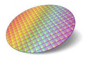
Semiconductor wafers are the basic material for manufacturing chips (as shown below). It is small but complicated. The production of wafer mainly involves 7 kinds of semiconductor materials and chemicals. The most important raw material for semiconductor integrated circuits is silicon, which is widely found in rocks and gravel in the form of silicate or silicon dioxide in nature. The manufacturing process of silicon wafers can be divided into three basic steps: silicon purification, monocrystalline silicon growth, and wafer formation. Apart from silicon, the manufacturing process of 200mm (8-inch) and below wafers is usually mainly made of aluminum, and the manufacture of 300mm (12-inch) wafer mostly uses advanced copper interconnection technology.

Semiconductor wafer

In conclusion, with more extensive use of semiconductor chips, the demand for aluminum, titanium, tantalum and copper, the four mainstream Anelva target, will also increase. There is currently no alternative to these target materials, either technically or economically, so, as I mentioned before,  they are important and irreplaceable.

Please visit https://www.sputtertargets.net/ for more information.

What should we do when the target is broken?

For most of the time, people consider the purity, and maybe the shape, of the sputtering target when they are purchasing the target materials. But one thing should not be ignored is the target bonding. Well, you think it unnecessary and costly? Then just think about what to do when your target is broken.broken target

Target bonding is necessary

Maybe you can use a copper plate to stick the broken pieces of the target and then polish the target so that the broken areas have minimum exposure to plasma. The second step is very important because the power would suddenly breakdown to zero when plasma strike to broken area of target. And obviously, the film quality will be affected if breakdown is frequent. Although it may help solve the problem when the target is broken, it is still a remedial measure. To avoid target from breaking, you need to give a target bonding service to the target. It is necessary for those brittle targets, and is not expensive compared with the losses of the broken target.

Continue reading “What should we do when the target is broken?”